Aakash iACST – NEET Repeater
Register for iACST. Get instant Scholarship on NEET Repeater Courses.


Ever wondered how the common electronic devices do their job, or the way the components, such as diodes, transistors, etc., operate in circuits? Class 12 Physics Chapter 14 - Semiconductor Electronics, Materials, Devices, and Simple Circuits gives the students an introduction to electronics. It is in this chapter that you will get to know about semiconductors, p-n junction diodes, and simple logic gates, e.g., AND, OR, and NOT. These topics are of vital importance in the study of the functioning of modern electronic devices and circuits.
This Story also Contains

The NCERT Exemplar Class 12 Physics Solutions Chapter 14 Semiconductor Electronics, Materials, Devices, and Simple Circuits, prepared by expert teachers in accordance with the latest CBSE syllabus, provide step-by-step solutions to all exemplar problems. The NCERT Exemplar Class 12 Solutions Physics Chapter 14 Semiconductor Electronics, Materials, Devices, and Simple Circuits encompasses MCQs, very short answer (VSA), short answer (SA) and long answer (LA) questions, which will ensure that the chapter is fully covered. The conceptual knowledge, practical application skills and good preparation of exams are among the reasons why practising these NCERT Exemplar Solutions Class 12 Physics questions helps students to prepare better for the CBSE board exams, JEE and NEET.
NCERT Exemplar Class 12 Physics Chapter 14: MCQ I give correct and conceptual solutions to multiple choice questions, as required by the NCERT pattern of Exemplar. These NCERT Exemplar Class 12 Physics Solutions Chapter 14 Semiconductor Electronics, Materials, Devices, and Simple Circuits assist the students in exercising their knowledge about semiconductors and electronic devices, besides effectively practising exam-based objective questions.
Question:1
The conductivity of a semiconductor increases with increase in temperature because
A. number density of free current carriers increases.
B. relaxation time increases.
C. both number density of carriers and relaxation time increase.
D. number density of current carriers increases, relaxation time decreases but effect of decrease in relaxation time is much less than increase in number density.
Answer:
The answer is option (d)Question:2
In Fig. 14.1, Vo is the potential barrier across a p-n junction, when no battery is connected across the junction

A. 1 and 3 both correspond to forward bias of junction
B. 3 corresponds to forward bias of junction and 1 corresponds to reverse bias of junction
C. 1 corresponds to forward bias and 3 corresponds to reverse bias of junction.
D. 3 and 1 both correspond to reverse bias of junction.
Answer:
Answer: The answer is option (b)Question:3
In Fig. 14.2, assuming the diodes to be ideal,

A. $D_1$ is forward biased and $D_2$ is reverse biased and hence current flows from A to B
B. D2 is forward biased and $D_1$ is reverse biased and hence no current flows from B to A and vice versa.
C. $D_1$ and $D_2$ are both forward biased and hence current flows from A to B.
D. $D_1$ and $D_2$ are both reverse biased and hence no current flows from A to B and vice versa.
Answer:
The answer is option (b)Question:4
A 220 V A.C. supply is connected between points A and B (Fig. 14.3). What will be the potential difference V across the resistor?

A. 220V
B. 110V
C. 0V
D. $220 \sqrt{2}V$
Answer:
As a p-n junction diode will conduct during the positive half cycle, only during the negative half cycle diode is reverse-biased. During this diode will not give any output, so the potential difference across the capacitor is the peak voltage of the given AC voltage
$V_{0}=V_{rms}\sqrt{2}=220 \sqrt{2}V$
Question:5
Hole is
A. an anti-particle of an electron.
B. a vacancy created when an electron leaves a covalent bond.
C. absence of free electrons.
D. an artificially created particle.
Answer:
The answer is option (b)Question:6
The output of the given circuit in Fig. 14.4.

A. would be zero at all times.
B. would be like a half wave rectifier with positive cycles in output.
C. would be like a half wave rectifier with negative cycles in output.
D. would be like that of a full wave rectifier.
Answer:
The answer is option (c)
would be like a half-wave rectifier with negative cycles in the output
Question:7
In the circuit shown in Fig. 14.5, if the diode forward voltage drop is 0.3 V, the voltage difference between A and B is

A. 1.3 V
B. 2.3 V
C. 0
D. 0.5 V
Answer:
The answer is option (b)Question:8
Truth table for the given circuit (Fig. 14.6) is

A.
|
A
|
B
|
C
|
|
0
|
0
|
1
|
|
0
|
1
|
0
|
|
1
|
0
|
1
|
|
1
|
1
|
0
|
|
A
|
B
|
C
|
|
0
|
0
|
1
|
|
0
|
1
|
0
|
|
1
|
0
|
0
|
|
1
|
1
|
1
|
|
A
|
B
|
C
|
|
0
|
0
|
0
|
|
0
|
1
|
1
|
|
1
|
0
|
0
|
|
1
|
1
|
1
|
|
A
|
B
|
C
|
|
0
|
0
|
0
|
|
0
|
1
|
1
|
|
1
|
0
|
1
|
|
1
|
1
|
0
|
Answer:
The answer is option (c)|
A
|
B
|
$\bar{A}$
|
C=A.B
|
d=$\bar{A}$.B
|
E=(C+D)
|
|
0
|
0
|
1
|
0
|
0
|
0
|
|
0
|
1
|
1
|
0
|
1
|
1
|
|
1
|
0
|
0
|
0
|
0
|
0
|
|
1
|
1
|
0
|
1
|
0
|
1
|
Get your results instantly with our calculator!
NCERT Exemplar Class 12 Physics Chapter 14: MCQ II is designed to challenge students' understanding of semiconductor electronics through thought-provoking and application-based multiple-choice questions. The solutions assist learners to master problem-solving skills, reason and critique concepts and prevent the common errors in the board and competitive examinations.
Question:9
When an electric field is applied across a semiconductor
A. electrons move from lower energy level to higher energy level in the conduction band.
B. electrons move from higher energy level to lower energy level in the conduction band.
C. holes in the valence band move from higher energy level to lower energy level.
D. holes in the valence band move from lower energy level to higher energy level.
Answer:
The answer is the option (a, c)Question:10
Consider an npn transistor with its base-emitter junction forward-biased and collector-base junction reverse-biased. Which of the following statements are true?.
A. Electrons crossover from emitter to collector.
B. Holes move from base to collector.
C. Electrons move from emitter to base.
D. Electrons from emitter move out of base without going to the collector.
Answer:
The answer is the option (a, c)Question:11
Figure 14.7 shows the transfer characteristics of a base-biased CE transistor. Which of the following statements are true?

A. At Vi = 0.4V, transistor is in active state.
B. At Vi = 1V, it can be used as an amplifier.
C. At Vi = 0.5V, it can be used as a switch turned off.
D. At Vi = 2.5V, it can be used as a switch turned on.
Answer:
The answer is the option (b, c, d)Question:12
In a npn transistor circuit, the collector current is 10mA. If 95 per cent of the electrons emitted reach the collector, which of the following statements are true?
A. The emitter current will be 8 mA.
B. The emitter current will be 10.53 mA.
C. The base current will be 0.53 mA.
D. The base current will be 2 mA.
Answer:
The answer is the option (b, c)Question:13
In the depletion region of a diode
A. there are no mobile charges
B. equal number of holes and electrons exist, making the region neutral.
C. recombination of holes and electrons has taken place.
D. immobile charged ions exist.
Answer:
The answer is the option (a, b, d)Question:14
What happens during the regulation action of a Zener diode?
A. The current in and voltage across the Zenor remains fixed.
B. The current through the series Resistance (Rs) changes.
C. The Zener resistance is constant.
D. The resistance offered by the Zener changes.
Answer:
The answer is the option (b,d)Question:15
To reduce the ripples in a rectifier circuit with capacitor filter
A. RL should be increased.
B. input frequency should be decreased.
C. input frequency should be increased.
D. capacitors with high capacitance should be used.
Answer:
The answer is the option (a, c, d)Question:16
The breakdown in a reverse-biased p–n junction diode is more likely to occur due to
A. large velocity of the minority charge carriers if the doping concentration is small.
B. large velocity of the minority charge carriers if the doping concentration is large.
C. strong electric field in a depletion region if the doping concentration is small.
D. strong electric field in the depletion region if the doping concentration is large.
Answer:
The answer is the option (a, d)
Reverse biasing is when the positive terminal of the battery is connected to the N-crystal, and the negative terminal of the battery is connected to the P-crystal.

In reverse biasing, ionisation takes place because the minority charge carriers get accelerated due to reverse biasing. They strike with the electrons, which in turn increase the number of charge carriers. And when the doping region is large, there will be a large number of ions in the depletion region. This will give rise to a strong electric field.
NCERT Exemplar Class 12 Physics Chapter 14:Very Short Answer gives us brief yet clear answers to the questions that ask one to test the major definitions and fundamental principles in the field of semiconductor electronics. These NCERT Exemplar Class 12 Physics Solutions Chapter 14 are perfect to revise in a short period and assist students in memorising great facts and rules effectively.
Question:17
Why are elemental dopants for Silicon or Germanium usually chosen from group XIII or group XV?
Answer:
Silicon and germanium are chosen as dopants because their size is compatible with the gaps in semiconductors. And they are even capable of forming covalent bonds.Question:18
Answer:
Sn is a conductor as it has an energy gap of 0 EV while C has an energy gap of 5.4 eV; therefore, it is an insulator. Si and Ge have energy gaps of 1.1 eV and 0.7 eV, which makes them semiconductors. The gaps in energy are related to their individual atomic size, which is responsible for making one an insulator, a conductor or a semiconductor.Question:19
Answer:
We cannot measure the potential barrier of a PN-junction by connecting a sensitive voltmeter across its terminals because in the depletion region, there are no free electrons and holes, and in the absence of forward biasing, PN-junction offers infinite resistance.Question:20
Draw the output waveform across the resistor (Fig.14.8).

Answer:
The diode acts as a half-wave rectifier; it offers low resistance when forward-biased and high resistance when reverse-biased.Question:21
The amplifiers X, Y and Z are connected in series. If the voltage gains of X, Y and Z are 10, 20 and 30, respectively and the input signal is 1 mV peak value, then what is the output signal voltage (peak value)
(i) If the DC supply voltage is 10V?
(ii) If the DC supply voltage is 5V?
Answer:
The ratio of the output signal voltage to the input signal voltage is known as the total voltage amplification.Question:22
Answer:
$(i) dc \: current\: gain: \beta_{dc}=\frac{i_{c}}{i_{b}}$Semiconductor Electronics, Materials, Devices, and Simple Circuits Class 12 NCERT Exemplar: Short Answer also has clear and well-structured solutions of questions that need brief explanations and the use of formulas. These NCERT Exemplar Class 12 Physics Solutions Chapter 14 assist the students in building conceptual knowledge, answering questions well, and performing well in exams.
Question:23
(a)

(b)

(i) Name the type of a diode whose characteristics are shown in Fig. 14.9 (A) and Fig. 14.9(B).
Answer:
i) Figure a) represents the characteristics of a Zener diode, and figure b) represents a solar cell.Question:24
Answer:
Question:25
Answer:
IbR1 + Vbe = Vbb
Base current = Ib = Vbb – Vbe/R1
Ib is inversely proportional to R1
Hence, if R1 is increased, then Ib gets reduced.
Question:26
Answer:
Here, the OR gate is used to explain the situation:|
A
|
B
|
Y=A+B
|
|
0
|
0
|
0
|
|
0
|
1
|
1
|
|
1
|
0
|
1
|
|
1
|
1
|
1
|
Question:28
Explain why elemental semiconductor cannot be used to make visible LEDs.
Answer:
In an elemental semiconductor, the bandgap is such that the emission is in the infrared region and not in the visible region.Question:29
Write the truth table for the circuit shown in Fig.14.11. Name the gate that the circuit resembles.

Answer:
|
A
|
B
|
V0=A.B
|
|
0
|
0
|
0
|
|
0
|
1
|
0
|
|
1
|
0
|
0
|
|
1
|
1
|
1
|
Question:30
Answer:
According to the problem, Power = 1 WattQuestion:31
Answer:
According to the problem forward biases resistance = $25 \Omega$ and reverse biases resistance=$\infty$Question:32
Answer:
According to the problem V1 =10V, Resistance RB=400k$\Omega$, VBE=0, VCE=0 and Rc=3k$\Omega$Semiconductor Electronics, Materials, Devices, and Simple Circuits Class 12 NCERT Exemplar: Long Answer contains stepwise answers to descriptive questions where reasoning at length and correct use of semiconductor and electronic devices concepts have to be put into practice. These NCERT Exemplar Class 12 Physics Chapter 14 Solutions will enable the students to grow to have a systematic method for solving problems and be able to work on high-mark questions when they come up in exams.
Question:33
Draw the output signals C1 and C2 in the given combination of gates (Fig. 14.15).

Answer:
|
A
|
B
|
C
|
D
|
E
|
F
|
G
|
H
|
I
|
C1
|
|
0
|
0
|
0
|
0
|
1
|
1
|
1
|
0
|
0
|
1
|
|
1
|
0
|
1
|
0
|
0
|
1
|
0
|
1
|
1
|
0
|
|
0
|
1
|
0
|
1
|
1
|
0
|
0
|
1
|
1
|
0
|
|
1
|
1
|
1
|
1
|
0
|
0
|
0
|
1
|
1
|
0
|
|
A
|
B
|
C
|
D
|
E
|
F
|
G
|
C2
|
|
0
|
0
|
0
|
0
|
1
|
1
|
1
|
0
|
|
1
|
0
|
1
|
0
|
0
|
1
|
1
|
0
|
|
0
|
1
|
0
|
1
|
1
|
0
|
1
|
0
|
|
1
|
1
|
1
|
1
|
0
|
0
|
0
|
1
|
Question:34
Consider the circuit arrangement shown in Fig 14.16 (a) for studying input and output characteristics of n-p-n transistor in CE configuration.

Select the values of RB and RC for a transistor whose VBE = 0.7 V, so that the transistor is operating at point Q as shown in the characteristics shown in Fig. 14.16 (b).

Given that the input impedance of the transistor is very small and VCC = VBB = 16 V, also find the voltage gain and power gain of the circuit, making appropriate assumptions.
Answer:
According to the problem at point Q, from graph $V_{BE}=0.7V,V_{CC}=V_{BB}=16V$ and $V_{CE}=8V$Question:35
Answer:
The waveform obtained from the circuit will be a sine wave with a little dip in the input wave.Question:36
Answer:
$n_{e}=N_{D}=10^{-6}\times 5 \times 10^{28}atoms/m^{3}\\ =5 \times 10^{22}/m^{3}$Question:37
An X-OR gate has following truth table:
|
A
|
B
|
Y
|
|
0
|
0
|
0
|
|
0
|
1
|
1
|
|
1
|
0
|
1
|
|
1
|
1
|
0
|
Answer:
XOR can be obtained by combining two NOT gates, two AND gates and one OR gate. The logical relation for the given table is as follows:Question:38
Consider a box with three terminals on top of it as shown in Fig.14.18 (a):

Three components namely, two germanium diodes and one resistor are connected across these three terminals in some arrangement.
A student performs an experiment in which any two of these three terminals are connected in the circuit shown in Fig. 14.18 (b).

The student obtains graphs of current-voltage characteristics for unknown combination of components between the two terminals connected in the circuit.
The graphs are
(i) when A is positive and B is negative

(ii) when A is negative and B is positive

(iii) When B is negative and C is positive

(iv) When B is positive and C is negative

(v) When A is positive and C is negative

(vi) When A is negative and C is positive

From these graphs of current–voltage characteristic shown in Fig. 14.18 (c) to (h), determine the arrangement of components between A, B and C.
Answer:
a) The n-side of the PN junction is connected to the A terminals, while the B is connected to the top-side of the PN junction.Question:39
Answer:
As we know, the base current is very small,
$
\begin{aligned}
& \quad I_C=I_E \\
& R_C=7.8 \mathrm{k} \Omega \\
& \text { from the fig. } I_C\left(R_c+R_E\right)+V_{C E}=12 \\
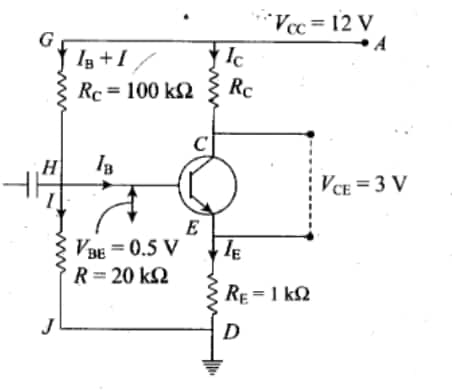
& \left(R_E+R_C\right) \times 1 \times 10^{-3}+3=12 \\
& \left(R_E+R_C\right)=9 \times 10^3=9 \mathrm{k} \Omega \\
& R_E=9-7.8=1.2 \mathrm{k} \Omega \\
& V_E=I_E \times R_E \\
& =1 \times 10^{-3} \times 1.2 \times 10^3=1.2 \mathrm{~V} \\
& \text { VoltageV } B=V_E+V_{B E}=1.2+0.5=1.7 \mathrm{~V} \\
& \text { Current } I=\frac{V_B}{20 \times 10^3}=\frac{1.7}{20 \times 10^3}=0.085 \mathrm{~mA} \\
& \text { Resistance } R_B=\frac{12-1.7}{\frac{I_C}{\beta}+0.085} \times 10^3=\frac{10.3}{0.01+0.085} \quad \text { [Given } \beta=100 \text { ] } \\
& =108 \mathrm{k} \Omega
\end{aligned}
$
Question:40
In the circuit shown in Fig.14.20, find the value of RC.

Answer:
Let us consider the circuit diagram to solve this problemModern electronics needs the knowledge of the behaviour of semiconductors and electronic devices. This chapter of NCERT Exemplar Class 12 Physics Chapter 14 is a compilation of the most crucial concepts and formulas in the study of diodes, transistors, logic gates and p-n junctions, which allow the student, both to revise effectively, to enhance the ability to solve problems, and to be able to use his knowledge in not only numerical but also theoretical questions in competitive and board examination.
1. Semiconductors
2. Intrinsic Semiconductor
3. Extrinsic Semiconductor
4. p-n Junction Diode
5. Forward Bias
6. Reverse Bias
7. Diode Equation
$
I=I_0\left(e^{V / V_T}-1\right)
$
Where $I_0$ is reverse saturation current, $V_T=k T / q$
8. Logic Gates
NCERT Exemplar Class 12 Physics Chapter 14 Solutions are developed to make the students realise the basic knowledge of semiconductors, electrical works and simple circuits in a straightforward and organised manner. These solutions help one to achieve conceptual clarity, application skills, and exam-oriented preparation for Class 12 Physics.
The step-by-step solutions will allow the students to realise the reasoning behind each solution as opposed to memorising the formula.
These exemplar questions are useful in enhancing analytical thinking and solving application-based problems involving electronics.
These are both theoretical and numerical problems that allow the students to strike a balance between conceptual and practical problem-solving.
They can be a very useful aid to prepare exams and assist students in predicting the question patterns and key points.
Solved examples help the students to be confident when interpreting circuit diagrams, logic gates, and the behaviour of electronic devices.
They can also be applied to competitive exams such as JEE and NEET competitive exams where semiconductor electronics is a significant aspect of the curriculum.
NCERT Exemplar Class 12 Physics Chapter-Wise Links are a good source that gives the students convenient access to the solutions of all the chapters of the Class 12 Physics syllabus. These connections facilitate saving on study time, facilitate a focused revision, and assist in a preparation that is efficient in board as well as competitive exams.
Frequently Asked Questions (FAQs)
Semiconductors are materials that have properties between conductors and insulators. They're super important because they power most modern electronic gadgets.
You’ll study diodes, transistors, logic gates, LEDs, and their working, applications, and how they’re used in electronic circuits.
Yes! The concepts you learn here are directly linked to real-world devices like smartphones, computers, calculators, and even traffic lights.
This chapter covers everything related to semiconductors like types, properties, junction transistors, diodes, logic gates, etc.
In NEET exam 2 to 3 questions are asked every year from the chapter Semiconductor Electronics. Mostly questions from both analog and digital electronics are included.
Students can get a better understanding of the concepts discussed in the chapter using NCERT Exemplar Solutions For Class 12 Physics Chapter 14, which in turn will be helpful for exams

On Question asked by student community
Hello Ananya,
Please specify the class for which you need the question papers. I am providing Class 10 and 12 papers.
Here are the links to the CBSE Half-yearly Question Papers (2025-2026).
Hello Ananya,
Please specify the class for which you need the question papers. I am providing Class 10 and 12 papers.
Here are the links to the CBSE Half-yearly Question Papers (2025-2026).
Hello Pawan,
CBSE Class 10 Mathematics 2026 and previous year question paper:
https://school.careers360.com/boards/cbse/cbse-class-10-question-paper-2026
CBSE Class 12 Mathematics 2026 and previous year question paper:
https://school.careers360.com/boards/cbse/cbse-previous-year-question-papers-class-12-maths
Hello Dharani,
Check the link below to download NCERT Class 12 previous year question papers in PDF format for all subjects.
https://school.careers360.com/boards/cbse/cbse-previous-year-question-papers-class-12
Hello Vipin,
Check the link below to download CBSE Class 12 question papers in PDF format for all subjects, including Mathematics.
https://school.careers360.com/boards/cbse/cbse-previous-year-question-papers-class-12
A block of mass 0.50 kg is moving with a speed of 2.00 ms-1 on a smooth surface. It strikes another mass of 1.00 kg and then they move together as a single body. The energy loss during the collision is
| Option 1)
|
Option 2)
|
| Option 3)
|
Option 4)
|
An athlete in the olympic games covers a distance of 100 m in 10 s. His kinetic energy can be estimated to be in the range
| Option 1)
|
Option 2)
|
| Option 3)
|
Option 4)
|
A particle is projected at 600 to the horizontal with a kinetic energy . The kinetic energy at the highest point
| Option 1)
|
Option 2)
|
| Option 3)
|
Option 4)
|
In the reaction,
| Option 1)
|
Option 2)
|
| Option 3)
|
Option 4)
|
How many moles of magnesium phosphate, will contain 0.25 mole of oxygen atoms?
| Option 1)
0.02 |
Option 2)
3.125 × 10⁻² |
| Option 3)
1.25 × 10⁻² |
Option 4)
2.5 × 10⁻² |
Register for iACST. Get instant Scholarship on NEET Repeater Courses.
Study at a world-renowned UK university in India | Admissions open for UG & PG programs.
Apply for UG & PG programmes from Victoria University, Delhi NCR Campus
Admissions open for UG & PG programs at Illinois Tech Mumbai
Apply for UG & PG courses at University of Aberdeen, Mumbai Campus
UG & PG Admissions open for CS/AI/Business/Economics & other programmes.