Aakash iACST – NEET Repeater
Register for iACST. Get instant Scholarship on NEET Repeater Courses.


Semiconductor Electronics is one of the most important chapters in Class 12 Physics, as it explains the working of modern electronic devices like smartphones, computers, LEDs, and solar cells. This chapter builds on the basic understanding of materials and introduces key concepts such as energy band theory, intrinsic and extrinsic semiconductors, doping, p-n junctions, diodes, transistors, rectifiers, and logic gates. It also helps students understand how these components are used in real-life electronic circuits.
This Story also Contains

In this article, students will get detailed NCERT solutions with step-by-step explanations, important formulas, extra practice questions, and Higher Order Thinking Skills (HOTS) problems. This complete coverage will help strengthen concepts, improve problem-solving skills, and prepare effectively for CBSE board exams as well as competitive exams like JEE and NEET.
The Class 12 Physics Chapter 14 - Semiconductor Electronics Materials Devices And Simple Circuit question answers offer detailed answers to each of the textbook questions, so that complicated concepts become easy to understand. These Class 12 physics chapter 14 Semiconductor Electronics Materials Devices And Simple Circuit questions answers are formatted according to the current CBSE syllabus and are very useful during revisions, examinations at the board level and even competitive applications like JEE/NEET examinations. They can also print the PDF to study offline and get last-minute reading practice.
The Class 12 Physics Chapter 14 - Semiconductor Electronics Materials Devices And Simple Circuit question answers (Exercise questions) offer step-by-step solutions to all questions in the textbook, and that is why it becomes easy to learn and apply the semiconductor concepts among students. Such Class 12 physics chapter 14 Semiconductor Electronics Materials Devices And Simple Circuit questions answers are accurate, clear, and they are used to prepare board exams as well as competitive exams such as JEE/NEET.
Q. 14.1 In an n-type silicon, which of the following statement is true:
(a) Electrons are majority carriers and trivalent atoms are the dopants.
(b) Electrons are minority carriers and pentavalent atoms are the dopants.
(c) Holes are minority carriers and pentavalent atoms are the dopants.
(d) Holes are majority carriers and trivalent atoms are the dopants.
Answer:
An N-type semiconductor has electrons as majority carriers and holes as minority carriers. It is formed when we dopea pentavalent impurity into a Silicon atom. Some pentavalent dopants are phosphorus, arsenic, and bismuth.
Hence, the correct option is C.
Q. 14.2 Which of the statements given in Exercise 14.1 is true for p-type semiconductors.
(a) Electrons are majority carriers and trivalent atoms are the dopants.
(b) Electrons are minority carriers and pentavalent atoms are the dopants.
(c) Holes are minority carriers and pentavalent atoms are the dopants.
(d) Holes are majority carriers and trivalent atoms are the dopants
Answer:
In a p-type semiconductor, holes are the majority carrier and electrons are the minority carrier. It is formed when a trivalent atom-like aluminium is doped in a silicon atom. Hence correct option for a p-type conductor would be (d).
(a) $(E_{g})_{Si} < (E_{g})_{Ge}< (E_{g})_{C}$
(b) $(E_{g})_{C} < (E_{g})_{Ge}> (E_{g})_{Si}$
(c) $(E_{g})_{C} > (E_{g})_{Si}> (E_{g})_{Ge}$
(d) $(E_{g})_{C} = (E_{g})_{Si}= (E_{g})_{Ge}$
Answer:
Since carbon is a non-metal, its energy band gap would be the highest, and the energy band gap of Ge would be the least, as it is a metalloid.
$(E_{g})_{C} > (E_{g})_{Si}> (E_{g})_{Ge}$
Hence correct option would be (c)
Q14.4 In an unbiased p-n junction, holes diffuse from the p-region to n-region beca
(a) free electrons in the n-region attract them
(b) they move across the junction by the potential difference.
(c) hole concentration in p-region is more as compared to n-region.
d) All the above
Answer:
Charge flows from the higher concentration to the lower concentration in a junction. In this case, holes are diffusing from the p-region to the n-region, and hence the concentration of holes is greater in the p-region.
and hence the correct option would be (c)
Q. 14.5 When a forward bias is applied to a p-n junction, it
(a) raises the potential barrier
(b) reduces the majority carrier current to zero.
(c) lowers the potential barrier.
(d) none of the above.
Answer:
When a p-n junction is forward biased, the negative voltage repels the electrons toward the junction and gives them the energy to cross the junction and combine with the hole, which is also being pushed by a positive voltage. This leads to a reduction in the depletion layer, which means a reduction in the potential barrier across the junction.
Hence correct option would be (c)
Answer:
As we know :
output frequency for a half-wave rectifier = input frequency, and hence output frequency in the half-wave rectifier will be 50Hz.
also, output frequency for full-wave rectifier = 2*(input frequency) and Hence output frequency in full-wave rectifier will be 2*50 = 100 Hz.
Class 12 Physics Chapter 14 - Semiconductor Electronics Materials Devices And Simple Circuit additional questions give students extra practice on concepts like p-n junctions, diodes, transistors, and logic gates. These questions go beyond the NCERT exercise, helping in deeper understanding and exam-focused preparation for boards as well as JEE/NEET.
Answer:
Given
the energy band gap of photodiode is 2.8eV.
wavelength = $\lambda$ = 6000nm = $6000*10^{-9}$
The energy of signal will be $\frac{hc}{\lambda }$
where c is speed of light(300000000m/s) , h is planks constant ( = $6.626 * 10^{-34}Js$ )
putting the corresponding value
The energy of signal = $\frac{(6.626 * 10^{-34} * 3*10^8)}{6000*10^{-9}}$
= $3.313*10^{-20}J$
= $0.207eV (since 1.6*10^{-20}= 1eV)$
The energy of the signal is 0.207eV, which is less than 2.8eV ( the energy and gap of the photodiode). Hence signal can not be detected by the photodiode.
Answer:
Given:
number of Silicon atoms per $m^{3}$ = $5\times 10^{28}.$
number of Arsenic atoms per $m^{3}$ = $5\times 10^{22}.$
number of Indium atoms per $m^{3}$ = $5\times 10^{20}$
number of thermally generated electrons $n_{i}=1.5\times 10^{16}\; m^{-3}.$
Now,
Number of electrons
$n_e =$ $5 * 10 ^{22}-1.5*10^{16}$ = $4.99*10^{22}(approx)$
number of holes is $n_h$
in thermal equilibrium
$n_h*n_e=n_i^2$
$n_h=n_i^2/n_e$
$n_h= (1.5*10^{16})^2/4.99*10^{22}$
$n_h= 4.51 * 10^9$
Now, since the number of electrons is higher than the number of holes, it is an n-type semiconductor.
Q.3 In an intrinsic semiconductor the energy gap $E_{g}$ is $1.2\; eV.$ Its hole mobility is much smaller than electron mobility and independent of temperature. What is the ratio between conductivity at $600K$ and that at $300K$ Assume that the temperature dependence of intrinsic carrier concentration $n_{i}$ is given by $n_{i}=n_{0}\; exp\left [ -\frac{E_{g}}{2K_{B}T} \right ]$ Where, $n_{0}$ is constant.
Answer:
Energy gap of given intrinsic semiconductor = E g = 1.2eV
temperature dependence of intrinsic carrier concentration $n_{i}$ is given by
$n_{i}=n_{0}\; exp\left [ -\frac{E_{g}}{2K_{B}T} \right ]$
Where is constant, $K_B$ is Boltzmann constant = $8.862 * 10^{-5}eV/K$ ,
T is temperature
Initial temperature = T1 = 300K
the intrinsic carrier concentration at this temperature :
$n_{i1} = n_0exp[\frac{-E_g}{2K_B*300}]$
Final temperature = T2 = 600K
the intrinsic carrier concentration at this temperature :
$n_{i2} = n_0exp[\frac{-E_g}{2K_B*600}]$
The ratio between the conductivities at 300K and at 600K is equal to the ratio of their intrinsic carrier concentration at these temperatures
$\frac{n_{i2}}{n_{i2}} = \frac{n_0exp[\frac{-E_g}{2K_B*600}]}{n_0exp[\frac{-E_g}{2K_B*300}]}$
$= exp\frac{E_g}{2K_B}[\frac{1}{300}-\frac{1}{600}]=exp[\frac{1.2}{2*8.62*10^{-5}}* \frac{2-1}{600}]$
$= exp[11.6] = 1.09 * 10^{5}$
Therefore, the ratio between the conductivities is $1.09 * 10^{5}$.
Q.4 In a p-n junction diode, the current I can be expressed as $I=I_{0}\; [exp \frac{eV}{K_{B}T}-1 ]$ where $I_{0}$ is called the reverse saturation current, V is the voltage across the diode and is positive for forward bias and negative for reverse bias, and $I$ is the current through the diode, $k_{B}$ is the Boltzmann constant $(8.6\times 10^{-5}eV/K)$ and $T$ is the absolute temperature. If for a given diode $I_{0}=5\times 10^{-12}A$ and $T=300\; K,$ then what will be the forward current at a forward voltage of $0.6\; V\; ?$
Answer:
As we have
$I=I_{0}\; [exp \frac{eV}{K_{B}T}-1 ]$
Here, $I_{0}=5\times 10^{-12}A$ , $T=300\; K,$ and , $k_{B}$ = Boltzmann constant = $(8.6\times 10^{-5}eV/K)$ $=(1.376*10^{-23}J/K)$
When the forward voltage is 0.6V:
$I=5*10^{-12}\;[ exp \frac{1.6*10^{-19}*0.6}{1.376*10^{-23}*300}-1 ]=0.0625A$
Hence, the forward current is 0.0625A
Q.5 In a p-n junction diode, the current I can be expressed as $I=I_{0}\; [exp \frac{eV}{K_{B}T}-1 ]$ where I0 is called the reverse saturation current, $V$ is the voltage across the diode and is positive for forward bias and negative for reverse bias, and $I$ is the current through the diode, $k_{B}$ is the Boltzmann constant $(8.6\times 10^{-5}\; eV/K)$ and $T$ is the absolute temperature. If for a given diode $I_{0}=5\times 10^{12}A$ and $T=300\; K,$ then what will be the increase in the current if the voltage across the diode is increased to $0.7 \; V?$
Answer:
As we have
$I=I_{0}\; [exp \frac{eV}{K_{B}T}-1 ]$
Here, $I_{0}=5\times 10^{-12}A$ , $T=300\; K,$ and , $k_{B}$ = Boltzmann constant = $(8.6\times 10^{-5}eV/K)$ $=(1.376*10^{-23}J/K)$
When the forward voltage is 0.7V:
$I=5*10^{-12}\;[ exp \frac{1.6*10^{-19}*0.7}{1.376*10^{-23}*300}-1 ]=3.029A$
When the forward voltage is 0.6V:
$I=5*10^{-12}\;[ exp \frac{1.6*10^{-19}*0.6}{1.376*10^{-23}*300}-1 ]=0.0625A$
Hence the increase in the forward current is
$I(whenv=0.7) - I(whenv=.6)$ $= 3.029- 0.0625 = 2.967A$
Q.6 In a p-n junction diode, the current I can be expressed as $I=I_{0}\; [exp \frac{eV}{K_{B}T}-1 ]$ where $I_{0}$ is called the reverse saturation current, $V$ is the voltage across the diode and is positive for forward bias and negative for reverse bias, and $I$ is the current through the diode, $k_{B}$ is the Boltzmann constant $(8.6\times 10^{-10}\; eV/K)$ and $T$ is the absolute temperature. If for a given diode $I_{0}=5\times 10^{-12}A$ and $T=300\; K,$ then what is the dynamic resistance?
Answer:
Dynamic Resistance = $\frac{voltage-change}{ current-change}$
Resistance change = 0.7 - 0.6 = 0.1
Current change = 2.967(calculated in prev question)
Therefore
, $Dynamic Resistance = \frac{0.1}{2.967} = 0.0337\Omega$
Answer:
As we have
$I=I_{0}\; [exp \frac{eV}{K_{B}T}-1 ]$
Here, $I_{0}=5\times 10^{-12}A$ , $T=300\; K,$ and , $k_{B}$ = Boltzmann constant = $(8.6\times 10^{-5}eV/K)$ $=(1.376*10^{-23}J/K)$
When reverse voltage is 1V, V = -1
$I=5*10^{-12}\;[ exp \frac{1.6*10^{-19}*(-1)}{1.376*10^{-23}*300}-1 ]\approx5\times10^{-12}$
When the reverse voltage is -2V:
$I=5*10^{-12}\;[ exp \frac{1.6*10^{-19}*(-2)}{1.376*10^{-23}*300}-1 ]\approx5\times10^{-12}$
In both cases, the current is very small and approximately equal to the reverse saturation current; hence, their difference is negligible, which causes the dynamic resistance of infinity.
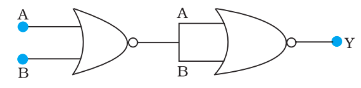
Q.8(a) You are given the two circuits as shown in Fig. Show that circuit acts as OR gate while the circuit
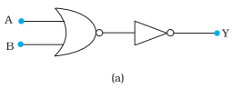
Answer:
Here, THE Input = A and B
Output = Y
The left part of the figure acts as a NOR, and the right part acts as a NOT Gate.
The output of NOR gate = $\overline{A+B}$
The output of the NOR gate would be the input of the NOT Gate, and hence
$\mathrm{Y}=\overline{\overline{A+B}}=\mathrm{A}+\mathrm{B}$
Hence, the figure functions like an OR Gate.
or compare the truth table by giving different inputs and observing the output
INPUTS | OUTPUT |
|---|---|
| A B | Y |
| 0 0 | 0 |
| 0 1 | 1 |
| 1 0 | 1 |
| 1 1 | 1 |
Q. 8(b) You are given the two circuits as shown in Fig. Show that circuit acts as AND gate.
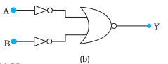
Answer:
The output of the NOT gate ( left part of the circuit) is the input of the NOR gate
Hence the output of total circuit Y = $\over(\overline A + \overline B)$
= $\overline{\overline A}.\overline{\overline B}$ $\overline{A+B}=\overline A. \overline B$
= $A*B$
Hence, the circuit functions as an AND gate.
or give the inputs 00,01,10,11, and observe the truth table
INPUTS | OUTPUT |
|---|---|
| A B | Y |
| 0 0 | 0 |
| 0 1 | 0 |
| 1 0 | 0 |
| 1 1 | 1 |
The truth table is the same as that of the AND gate
Q.9 Write the truth table for a NAND gate connected as given in the figure.
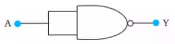
Hence, identify the exact logic operation carried out by this circuit.
Answer:
Here, A is both the input of the NAND gate and hence, Output Y will be
$Y = \overline {A*A}$
$Y = \overline {A} + \overline A$
$Y = \overline {A}$
Hence circuit functions as a NOT gate.
The truth table for the given figure:
| Input | Output |
| A | Y |
| 0 | 1 |
| 1 | 0 |
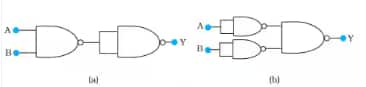
Answer:
a)
A and B are inputs of a NAND gate, and the output of this gate is the input of another NAND gate, so,
Y = $\over(\overline {A.B})(\overline {A.B})$
Y= $\over(\overline {A.B})$ $+$ $\over(\overline {A.B})$
Y= $AB$
Hence, this circuit functions asan AND gate.
b)
A is input to the NAND gate whose output goes to the rightmost NAND gate. Also, B is input to the NAND gate whose output goes to the rightmost NAND gate.
Y = $\over \overline A .\overline B$
Y = $\over\overline A .$ + $\over\overline B.$
Y = A + B
Hence, the circuit functions as an OR gate.
Alternative method
fig. a
Construct the truth table by giving various inputs and observing the output
| INPUT | INTERMEDIATE OUTPUT | OUTPUT |
| 00 | 1 | 0 |
| 01 | 1 | 0 |
| 10 | 1 | 0 |
| 11 | 0 | 1 |
The above truth table is the same as that of an AND gate
fig. b
| INPUTS | OUTPUT |
| 00 | 0 |
| 01 | 1 |
| 10 | 1 |
| 11 | 1 |
The above truth table is the same as that of an OR gate
Answer:
A and B are the inputs of a NOR gate, and the Output of this NOR gate is the Input of another NOR gate whose Output is Y. Hence,
Y = $\over(\overline{A+B} + \overline{A+B})$
Y = $\over\overline {A+B}$ . $\over\overline {A+B}$
Y = A + B
Hence Circuit behaves as an OR gate.
Truth table
| INPUTS | OUTPUT |
| 00 | 0 |
| 01 | 1 |
| 10 | 1 |
| 11 | 1 |
Answer:
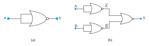
a)
A are the two inputs of the NOR gate, and hence Output Y is:
Y = $\overline {A+A}$
Y = $\overline {A}$
Hence circuit functions as a NOT gate.
TRUTH TABLE:
| INPUT | OUTPUT |
| 0 | 1 |
| 1 | 0 |
b) A is the two inputs of a NOR gate whose output(which is $\overline {A}$ ) is the one input of another NOR gate. B is the two inputs of the NOR gate whose output (which is $\overline {B}$ ) is the input of another NOR gate. Hence,
Y = $\over\overline {A} + \overline {B}$
Y = $\over\overline {A}$ . $\over\overline {B}$
Y = A.B
Hence, it functions as an AND gate.
TRUTH TABLE:
| INPUTS | OUTPUT |
| 00 | 0 |
| 01 | 0 |
| 10 | 0 |
| 11 | 1 |
Get your results instantly with our calculator!
Class 12 Physics NCERT Chapter 14 HOTS (Higher Order Thinking Skills) Questions challenge students to apply semiconductor concepts like diode characteristics, transistor action, rectifiers, and logic circuits in tricky problem-solving. These questions enhance critical thinking and analytical skills, making students better prepared for competitive exams and advanced applications.
Q1:
For an amplifier (NPN), VBC = 0, $\beta=50$, IC = 2.475 mA. Then the value of IB = ?
Answer:
As we learn
Relation between emitter current, Base current, and collector current -
$
I_E=I_B+I_C
$
- wherein
$I_E=$ Emitter Current
$I_B=$ Base Current
$I_C=$ Collector Current
$
I_B=\frac{I_C}{\beta}=\frac{2.475}{50}=49.5 \mathrm{~mA}
$
Q2:
A Si diode has a saturation current of 10-7 A. Calculate the junction current for a forward bias of 0.7 V and 300 k (y = 2 for Si and V = 26 mV)
Answer:
As we learn,
Relation between current I & Voltage V -
$I=I_0\left(e^{\frac{c v}{K T}}-1\right)$
- wherein
K = Boltzmann constant
I0 = reverse saturation current
In forward bias
$e^{\frac{r v}{K T}}>>1$
Then, the forward biasing current is
$I=I_0 \cdot e^{\frac{c v}{K T}}$
$I=I_0\left(e^{\frac{\mathrm{cv}}{K T}}-1\right)=I_0\left(e^{\frac{v}{y+V_T}}-1\right)=10^{-7}\left(\frac{0.7}{2 \times 26}-1\right)=70 \mathrm{~mA}$
Q3:
Find the current through the circuit for Si diode`

Given that -
Knee voltage for Ge is 0.3 V
Knee voltage for Si is 0.7 V
Answer:
Knee voltage of P-N junction -
It is defined as that forward voltage at which the current through the junction starts rising rapidly with an increase in voltage.
Knee voltage for Ge is 0.3 V
Knee voltage for Si is 0.7 V
$I=\frac{3.4-0.7}{600}=\frac{2.7}{600}=4.5 \mathrm{~mA}$
Q4:

The truth table for the above logic circuit is the same as that of :
Answer:
As we learn
NOR Gate -
NOT + OR Gate

- wherein
$Y=\overline{A+B}$
A and B are input
Y is output

The output (y) of two input (A, B) NOR gates is :
$Y=\overline{A+B}$
Q5:
For the circuit shown current through 1.5K$\Omega$ is:

Answer:
As we learn
Zener diode can operate continuously without being damaged in the region of reverse bias
- wherein
1) It acts as a voltage regulator
2) In forward biasing, it acts as an ordinary diode.
$I_L=\frac{V_Z}{1.5 \mathrm{~K}}=\frac{6}{1.5 \times 10^3}=4 \mathrm{~mA}$
Class 12 Physics Chapter 14 - Semiconductor Electronics Materials Devices And Simple Circuit introduces the working principles of semiconductors, diodes, transistors, rectifiers, and logic gates that form the backbone of modern electronics. Understanding these topics helps students connect theory with real-world applications in devices like mobiles, LEDs, and computers.
To answer the questions on Semiconductor Electronics, it is essential to have a good understanding of such concepts as p-n junctions, diodes, transistors and logic gates. Using a well-defined step-by-step approach, students will be able to work both theoretically and numerically with a sense of confidence. This approach is useful in achieving good scores in board exams and also JEE/NEET, where precision and usage of concepts are important.
Current gain in a transistor: $\beta=\frac{I_C}{I_B}$
$
\left.I_E=I_B+I_C \text { (Emitter current }=\text { Base }+ \text { Collector }\right)
$
Chapter 14 of Class 12 Physics NCERT Solutions: Semiconductor Electronics: Materials, Devices and Simple Circuits is very important because this chapter presents the students with the fundamentals of modern electronics and solid-state devices. It links theoretical physics and actual electronics of the real world.
The chapter Semiconductor Electronics: Materials, Devices and Simple Circuits assists students in their comprehension of the microscopic charge behaviour that results in the operation of the electronic devices that they use in their day-to-day activities. With the support of NCERT Solutions for Class 12 Physics Chapter 14, learners move from basic material properties to the working of electronic devices in a logical and application-oriented manner.
Also read :
Although the basics of semiconductors, diodes, and transistors are taught in NCERT, students who are going to take on the JEE and NEET exams must take it a step further. Competitive exams require a more in-depth problem-solving, application-based numerals, and exposure to the conceptual questions that are tricky. Comparison of NCERT vs. JEE/NEET requirements can be used to determine the additional topics and practice to achieve success in the exams.
NCERT Solutions of Class 12 Physics contain step-by-step explanations on each chapter that make the complicated theories simple. These solutions have been prepared according to the new CBSE syllabus and are quite beneficial in preparation for board exams, JEE and NEET. The following links lead to chapter-wise solutions that the students can download and revise to access knowledge.
Frequently Asked Questions (FAQs)
They give step-by-step explanations to make the not-so-easy concepts easier and to solve questions in exercises in a straightforward manner.
Yes, NCERT Solutions is enough to pass boards yet however having practice and doing sample papers will increase your mark.
Absolutely! Most of the questions in JEE and NEET are directly and indirectly linked to the NCERT concepts; hence, these solutions assist in building a great foundation.
Yes, all NCERT Solutions in each Chapter can be downloaded as PDFs to study and revise.
You should read the NCERT textbook, go over the NCERT Solutions to clear any confusion, then do previous year papers and mock tests.
Writing mathematical equations for p-n junctions or transistor circuits, identifying known variables, and changing values to the appropriate units are only a few of the detailed approaches that solutions provide. Frequent use of these simple methods results in quicker computations and fewer careless mistakes in time-bound examinations.
Questions typically contain definitions, working principles of the devices, label diagrams, logic gates and basic circuit based numericals.
Types of semiconductors, p-type versus n-type, forward versus reverse biasing and transistor configuration are often confused by students.

On Question asked by student community
Hello Ananya,
Please specify the class for which you need the question papers. I am providing Class 10 and 12 papers.
Here are the links to the CBSE Half-yearly Question Papers (2025-2026).
Hello Ananya,
Please specify the class for which you need the question papers. I am providing Class 10 and 12 papers.
Here are the links to the CBSE Half-yearly Question Papers (2025-2026).
Hello Pawan,
CBSE Class 10 Mathematics 2026 and previous year question paper:
https://school.careers360.com/boards/cbse/cbse-class-10-question-paper-2026
CBSE Class 12 Mathematics 2026 and previous year question paper:
https://school.careers360.com/boards/cbse/cbse-previous-year-question-papers-class-12-maths
Hello Dharani,
Check the link below to download NCERT Class 12 previous year question papers in PDF format for all subjects.
https://school.careers360.com/boards/cbse/cbse-previous-year-question-papers-class-12
Hello Vipin,
Check the link below to download CBSE Class 12 question papers in PDF format for all subjects, including Mathematics.
https://school.careers360.com/boards/cbse/cbse-previous-year-question-papers-class-12
A block of mass 0.50 kg is moving with a speed of 2.00 ms-1 on a smooth surface. It strikes another mass of 1.00 kg and then they move together as a single body. The energy loss during the collision is
| Option 1)
|
Option 2)
|
| Option 3)
|
Option 4)
|
An athlete in the olympic games covers a distance of 100 m in 10 s. His kinetic energy can be estimated to be in the range
| Option 1)
|
Option 2)
|
| Option 3)
|
Option 4)
|
A particle is projected at 600 to the horizontal with a kinetic energy . The kinetic energy at the highest point
| Option 1)
|
Option 2)
|
| Option 3)
|
Option 4)
|
In the reaction,
| Option 1)
|
Option 2)
|
| Option 3)
|
Option 4)
|
How many moles of magnesium phosphate, will contain 0.25 mole of oxygen atoms?
| Option 1)
0.02 |
Option 2)
3.125 × 10⁻² |
| Option 3)
1.25 × 10⁻² |
Option 4)
2.5 × 10⁻² |
Register for iACST. Get instant Scholarship on NEET Repeater Courses.
Study at a world-renowned UK university in India | Admissions open for UG & PG programs.
Apply for UG & PG programmes from Victoria University, Delhi NCR Campus
Admissions open for UG & PG programs at Illinois Tech Mumbai
Apply for UG & PG courses at University of Aberdeen, Mumbai Campus
UG & PG Admissions open for CS/AI/Business/Economics & other programmes.