Search Colleges, Exams, Schools & more


Login
NCERT Class 12 Physics Chapter 14 Notes Semiconductor Electronics Materials Devices and Simple Circuits - Download PDF
Have you ever asked yourself how billions of instructions are processed in a fraction of a second by your smartphone or laptop? The key is in small electronic parts such as diodes and transistors, the atoms of modern technology. Chapter 14: Semiconductor Electronics - Materials, Devices, and Simple Circuits covers these fundamentals in detail, and NCERT Class 12 Physics Chapter 14 Notes Semiconductor Electronics: Materials, Devices and Simple Circuits available through Careers360 make them simple and complete to acquire.
This Story also Contains
- Semiconductor Electronics: Materials, Devices and Simple Circuits Class 12 Notes: Download PDF
- NCERT Class 12 Physics Chapter 14 Notes
- Semiconductor Devices: Previous Year Question and Answer
- Importance of NCERT Class 12 Physics Chapter 14 Notes
- NCERT Class 12 Notes Chapterwise
- NCERT Books and Syllabus
This chapter presents the students with metals, insulators, and semiconductors and their behaviour in terms of the band theory of solids. Intrinsic and extrinsic semiconductors, p-n junctions, diodes, and logic gates are included as the core concepts and explained in a straightforward manner with diagrams and examples to make the concepts easier to understand. These Chapter 14 NCERT notes of Class 12 are not only invaluable to students studying not just to take competitive exams such as CBSE board exams, but also to take competitive exams such as JEE, NEET. They give a good basis in semiconductor physics and electronic circuits to enable students to understand the principles behind modern electronic devices and enable them to solve difficult problems in their exams.
Also, students can refer,
Semiconductor Electronics: Materials, Devices and Simple Circuits Class 12 Notes: Download PDF
Get all the significant concepts at a single location and download the NCERT Class 12 Physics Chapter 14 Notes PDF on Semiconductor Electronics: Materials, Devices and Simple Circuits. Such notes include p-n junctions, diodes, transistors, intrinsic and extrinsic semiconductors, and applications of these in electronic devices. The PDF is perfect when it comes to using the CBSE board exams and the competitive exams such as the JEE and NEET since it has brief explanations, diagrams, formulas and solved problems, and can be revised anywhere at any time.
NCERT Class 12 Physics Chapter 14 Notes
The Semiconductor Electronics: Materials, Devices and Simple Circuits Class 12 Note give a straightforward explanation of the semiconductors, p-N junction, diodes, and transistors. These notes describe the basic concepts of electronic devices and their practical use, and so students find it easier to prepare to take the CBSE board exams and other competitive exams, including the JEE and NEET.
History of Electronic Devices
Earlier electronic devices were made up of vacuum tubes or valves.
-
The evolution of vacuum tubes started with diodes and proceeded to date with triode, tetrode and pentode.
-
Valves are responsible for controlling the flow of electrons. In diodes, there used to be two electrodes i.e. cathode and anode.
-
Similarly, a triode used to have three electrodes i.e. cathode, grid and anode and a tetrode used to have four electrodes i.e. anode, two grids and cathode and a pentode used to have five electrodes i.e. anode, three grids and cathode.
-
In vacuum tubes, the electrons are produced by heating the cathode using a low-tension battery. The vacuum helps the electron not to lose its energy by collision with air molecules in its way.
-
The disadvantages of vacuum tube devices are that they used to be
- Huge
- Operate at high voltages
- Consume a lot of power
- Have a restricted life
- Low responsibility
Classification of Metals, Semiconductors and Insulators
According to the physical phenomenon, we will simply tell whether or not it is classified as metals, semiconductors or insulators.
The electrical physical phenomenon is mostly diagrammatic by σ, whereas the reciprocal ofthe physical phenomenon is electric resistance and is diagrammatic by ρ = 1/σ
Metals
Metals have high physical properties and low electrical resistance
The order of ρ is 10-2 to 10-8 Ω m
The order of σ is 102 to 108 S/m
Semiconductors
They have conductivity and resistivity in between metals and insulators.
The order of ρ is 10-5 to 10-6 Ω m
The order of σ 105 to 106 S/m
Insulators
They have high resistivity and hence low conductivity.
The order of ρ is 10-11 to 10-19 Ω m
The order of σ 102 to 1019 S/m
Classification of semiconductors
The semiconductors can be classified into two types i.e. Elementary kind semiconductor and compound kind semiconductor.
Elementary type semiconductor
These types of semiconductors are available in natural form, for exampl,e Silicon (Si) and germanium (Ge)
Compound-type semiconductor
When semiconductors are made by compounding the metals, compound-type semiconductor is obtained. Further, they can be classified into
-
Inorganic semiconductors like CdS, GaAs, etc.
-
Organic semiconductors like Anthracene, doped phthalocyanines
-
Organic polymers – Polypyrrole, polyaniline, polythiophene
Band Theory of Solids
The energy levels of the atom form a nonstop band, wherever the electrons move. This is known as the band theory of solids.
-
In an atom, the protons and the neutrons constitute the central part called the nucleus.
-
The electrons revolve around the nucleus in definite orbits.
-
The orbits are named as 1s, 2s, 2p, 3s, 3p, 3d etc. each of which features totally different energy.
-
All electrons of the same orbit will have the same energy.
-
The electrons within the innermost orbits that are fully crammed are valence electrons, whereas the electrons within the outermost orbit that don't fully fill that shell are known as conduction electrons.
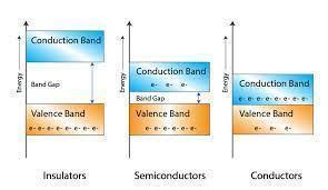
Classification on the Basis of Energy Bands
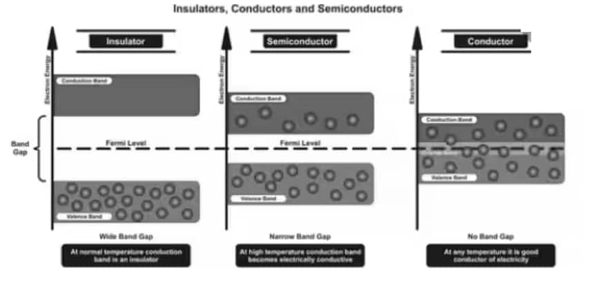
Depending upon the relative position of the valence band and the conduction band, the solids are classified into three categories i.e. conductors, insulators and semiconductors.
Conductors
-
The conduction band and the valence band overlap one another, and there's no impermissible energy bandgap in between.
-
The electrons from the valence band can easily move into the conduction band.
-
A large number of electrons are available for conduction.
-
The resistance of such materials is low, but the conductivity is high.
Insulators
-
In insulators, there is a large energy gap between the valence band and the conduction band.
-
The energy gap is very high, such that the electrons from the valence band cannot move to the conduction band by thermal excitation.
-
As there are no electrons in the conduction band, electrical conduction is not possible.
Semiconductors
-
A finite but small energy gap exists between the valence band and the conduction band.
-
At room temperature, some of the electrons from the valence band acquire energy and move into the conduction band.
-
At high temperatures, semiconductors have conductivity. The resistance is not as high as in insulators.
-
Semiconductors are of two types: Intrinsic and Extrinsic Semiconductor
Intrinsic Semiconductor
It is a pure semiconductor. Silicon and germanium are the most common examples of intrinsic semiconductors. Both these semiconductors are most frequently used in the manufacturing of transistors, diodes and other electronic components.
Both Si and Ge have four valence electrons. In its crystalline structure, every Si or Ge atom tends to share one of its four valence electrons with each of its four nearest neighbour atoms, and also to take a share of one electron from each such neighbour, as shown in the figure below. This shared pair of electrons is called a Covalent bond or a Valence bond.
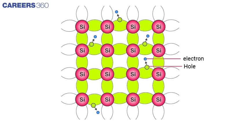
The above figure shows the structure with all bonds intact (i.e. no bonds are broken). This is possible only at low temperatures. As the temperature increases, more thermal energy becomes available to these electrons and some of these electrons may break away from the conduction band, becoming free electrons and creating a vacancy in the band. This vacancy with an effective positive electronic charge is called a hole.
In intrinsic semiconductors, the number of free electrons ( ne ) is equal to the number of holes ( nh )
i.e
Semiconductors possess the unique property in which, apart from electrons, the holes also move. The free electron moves completely independently as a conduction electron and gives rise to an electron current, Ie under an applied electric field. While under an electric field, these holes move towards the negative potential, generatinga hole current (Ih).
Hence, the total current (I) is given as
Apart from the process of generation of conduction electrons and holes, a simultaneous process of recombination occurs in which the electrons recombine with the holes. At equilibrium, the rate of generation is equal to the rate of recombination of charge carriers.


The conductivity of an intrinsic semiconductor at room temperature is very low. As such, no important electronic devices can be developed using these semiconductors. Hence, there is a necessity to improve their conductivity. This can be done by making use of impurities.
Extrinsic Semiconductor
An extrinsic semiconductor is a semiconductor doped by a specific impurity which is able to deeply modify its electrical properties, making it suitable for electronic applications. The deliberate addition of a desirable impurity is called doping and the impurity atoms are called dopants.
n-type Semiconductor
When a pentavalent impurity is added to an intrinsic or pure semiconductor, then it is said to be an n-type semiconductor. Pentavalent impurities such as phosphorus, arsenic, antimony, etc are called donor impurities.
The four valence electrons of each phosphorus atom form 4 covalent bonds with the 4 neighbouring silicon atoms. The free-electron (fifth valence electron) of the phosphorus atom is not involved in the formation of covalent bonds. This shows that each phosphorus atom donates one free electron. Therefore, all the pentavalent impurities are called donors.
So, there is a donor energy level between the valence band and the conduction band. Just below the conduction band.
The number of free electrons depends on the amount of impurity (phosphorus) added to the silicon.

In an n-type semiconductor, conduction is mainly due to the motion of free electrons.
In an n-type semiconductor, the population of free electrons is more, whereas the population of holes is less (i.e. ne >>nh). In an n-type semiconductor, free electrons are called majority carriers and holes are called minority carriers.
p-type semiconductor
When the trivalent impurity is added to an intrinsic semiconductor, then it is said to be a p-type semiconductor. Trivalent impurities such as Boron (B), Gallium (G), Indium(In), Aluminium(Al), etc are called acceptor impurities.
The three valence electrons of each boron atom form 3 covalent bonds with the 3 neighbouring silicon atoms. For the fourth covalent bond, only the silicon atom contributes one valence electron. Thus, the fourth covalent bond is incomplete with the shortage of one electron. This missing electron is called a hole.
This shows each boron atom accepts one electron to fill the hole. Therefore, all the trivalent impurities are called acceptors. So there is an acceptor energy level just above the valence band. A small addition of impurity (boron) provides millions of holes.

In a p-type semiconductor, conduction is mainly due to the motion of holes in the valence band.
In a p-type semiconductor, the population of free electrons is less, whereas the population of holes is more (i.e nh >>ne)
In a p-type semiconductor, holes are called majority carriers and free electrons are called minority carriers.
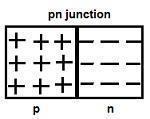
p-n Junction Formation
-
A p-n junction is the basic building block of many semiconductor devices like diodes, transistors, etc.
-
The holes are the majority carriers in the p-type semiconductor, whereas the electrons are the majority carriers in the n-type semiconductor.
-
In n-type semiconductors, the concentration of electrons is more as compared to the concentration of holes. Similarly, in p-type semiconductors, the concentration of holes is more as compared to the concentration of electrons.
-
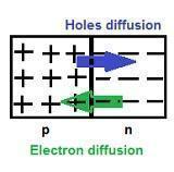
Diffusion is the first process that occurs in the p-n semiconductor.
-
In the formation of the p-n junction, due to the concentration gradient across the p and the n sides, there is the diffusion of electrons from the n region and therefore the holes are diffused from the p region to the n region.
Diffusion Current
-
It is due to the motion of charge carriers due to the difference in concentration in two regions of the p-n junction, across the junction.
-
The diffusion leaves behind a positive charge on the n-side close to the junction. This positive charge, known as an ionised donor, is immobile due to bonding with the surrounding atoms.
-
Similarly, in the p-region near the junction, there is a negative charge or acceptor ions that are immobile.
Depletion region formation
-
The space charge region on both sides of the p-n junction is devoid of any charge carriers and has immobile ions.
-
Due to this, it results in the formation of a depletion region near the junction.
Field setup
-
As the depletion region is formed, it results in setting up a field at the junction.
-
The field along the junction acts like a fictitious battery that is connected across the junction with a positive terminal connected to the n-region.
Barrier creation
-
The electric field at the junction sets a barrier opposing further diffusion of majority charge carriers through the junction.
-
Thus, the barrier that is created at the junction prevents further diffusion.
-
Width of the barrier:- The distance from one side of the barrier to the other is called the width of the barrier.
-
Height of the barrier:- The potential difference from one side of the barrier to the other side is known as the height of the barrier.
Drift current
-
Since the electric field is developed at the junction, the electrons from the p-region move to the n-region. Similarly, the hole from the n-region moves to the p-region. Due to this drift current is produced.
Drift current Vs Diffusion current
-
The drift current is in the opposite direction to the diffusion current.
-
At a particular stage, the drift current becomes equal to the diffusion current.
-
This stage is set to be in an equilibrium state when no current flows across the p-n junction.
-
The Potential barrier is maximum and is equal to VB.
-
Thus, a p-n junction is formed, and under equilibrium, there is no net current.
-
The electrons or holes move a large distance before the collision with another electron or hole when the doping concentration is small.
-
As a result, the width of the p-n junction becomes large.
-
On the contrary, the electric field becomes small as the width of the p-n junction increases.
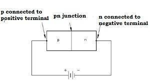
Forward Biasing
-
When we connect the positive terminal of the external battery to the p-side and the negative terminal of the external battery to the n-side, the p-n junction is said to be forward-biased.
-
The direction of the applied voltage V is in the opposite direction to the potential barrier setup at the junction.
-
The depletion layer width decreases, and the barrier height is reduced. The effective barrier height beneath forward bias is VB-V.
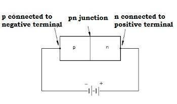
Reverse Biasing
-
When we connect the positive terminal of the external battery to the n-side and the negative terminal of the external battery to the p-side, then the p-n junction is said to be reverse-biased.
-
The applied voltage is in the same direction as the barrier potential.
-
The barrier height increases and the depletion region widens due to a change in the electric field.
-
The effective barrier height is VB+V
.png)
Application of a Junction Diode as a Rectifier
The rectifier is a device used for converting alternating current or voltage into direct current or voltage.
-
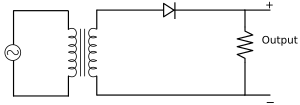
Half-wave rectifier: The figure below represents the half-wave circuit:
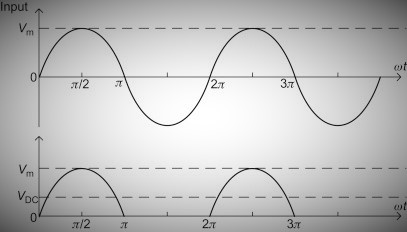
The input and output waveforms of a half-wave rectifier are as follows:
-
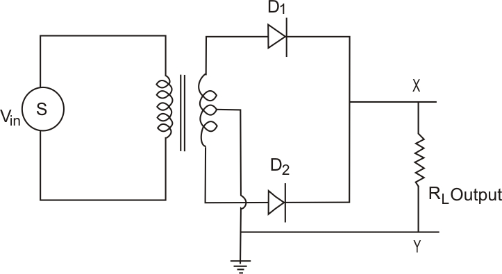
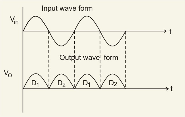
Full-wave rectifier: The figure below represents the half-wave circuit-
-
A p-n junction diode is used both as a half-wave and a full-wave rectifier.
-
The resistance of a p-n junction diode is low when forward-biased and is high when reverse-biased.
Confused between CGPA and Percentage?
Get your results instantly with our calculator!
💡 Conversion Formula used is: Percentage = CGPA × 9.5
Semiconductor Devices: Previous Year Question and Answer
Q.1 Draw the energy band diagrams for p-type and n-type semiconductors. Depict the donor/acceptor energy levels in these diagrams and write their significance.
Answer:
The energy band diagram of n-type, Semiconductor at temperature (left figure)
The energy band diagram of p-type, Semiconductor at temperature (right figure)

Q.2 Explain the two processes which occur during the formation of a p-n junction diode. Hence, define the terms (i) depletion region and (ii) potential barrier.
Answer:
The two processes are
- Diffusion
- Drift
Due to the concentration gradient of electrons, electrons diffuse from n to p and holes diffuse from p to n.
Due to the diffusion, an electric field is developed across the junction. Due to this electric field, electron moves from the p to the n side and holes from the n to the p side. The current due to this flow of charge is known as the drift current.
After some time, the diffusion current equals the drift current and further flow of charge is stopped.
(i) Depletion Region -
It is the space charge region on either side of the junction, which is depleted of free charges,
(ii) Potential barrier-
The potential difference developed across the junction and opposes the diffusion of charge and brings the equilibrium condition, is known as the potential barrier.
Q.3 In Fig. Vo is the potential barrier across a p-n junction when no battery is connected across the junction.

(1) 1 and 3 both correspond to the forward bias of the junction.
(2) 3 corresponds to forward bias of the junction and 1 corresponds to reverse bias of the junction.
(3) 1 corresponds to forward bias and 3 corresponds to reverse bias of the junction.
(4) 3 and 1 both correspond to reverse bias of the junction.
Answer:
The height of a potential barrier increases when the p-n junction is biased forward, and it opposes the potential barrier junction. But if p-n is reverse biased, the potential barrier junction is supported, which increases the potential barrier.
Hence, the answer is option (2).
Importance of NCERT Class 12 Physics Chapter 14 Notes
Fundamentals of Modern Electronics: Semiconductors, diodes and transistors
- To understand how daily devices such as smartphones, computers and light-emitting diodes operate, it is important to have an understanding of these devices.
Exam Preparation
- It has been a common question in board exams of CBSE, and a good understanding of the concepts leads to understanding both the theoretical and numerical parts of the question well.
Competitive Exam Advantage
- p-n junctions and logic gates, as well as intrinsic/extrinsic semiconductors, are important to JEE, NEET, and other engineering/medical entrance exams.
Conceptual Clarity
- The notes are organised to simplify complicated issues such as band theory of solids, diode characteristics, and transistor operation, enabling ease and faster learning.
Application-Oriented Learning
- Students are able to bridge theory and practical application and increase problem-solving and practical understanding.
Concise, yet Friendly
- The notes are written in brief explanations, diagrams and formulas and are perfect for revision prior to examinations.
Step To More Advanced Studies
- The mastery of this chapter provides a solid foundation to further-level electronics, physics, and engineering concepts in other studies.
NCERT Class 12 Notes Chapterwise
NCERT Class 12 Notes Chapterwise provide well-structured, simplified, and exam-oriented study material for every Physics chapter. These notes help students grasp key concepts, formulas, and derivations easily, making them perfect for CBSE Board exam revision as well as competitive exams like JEE and NEET.
|
NCERT Class 12 Physics Chapter 14 Notes |
Subject Wise NCERT Exemplar Solutions
- NCERT Exemplar Class 12 Solutions
- NCERT Exemplar Class 12 Maths
- NCERT Exemplar Class 12 Physics
- NCERT Exemplar Class 12 Chemistry
- NCERT Exemplar Class 12 Biology
Subject Wise NCERT Solutions
NCERT Books and Syllabus
Frequently Asked Questions (FAQs)
Q: What is a semiconductor?
A:
A semiconductor is a material whose electrical conductivity lies between that of a conductor and an insulator. Silicon and germanium are common examples.
Q: Is it necessary to memorize all logic gate truth tables?
A:
Yes, it’s important to understand and memorize the basic truth tables for gates like AND, OR, NOT, NAND, NOR, XOR, as they are commonly asked.
Q: Is this chapter important for JEE or NEET?
A:
Definitely! JEE and NEET include theory-based and application-level MCQs from this chapter, especially on semiconductors, diodes, and logic gates.
Q: What is a p-n junction?
A:
It’s the boundary formed between p-type and n-type semiconductors. It is the basic building block of devices like diodes and transistors.
Q: What is doping and why is it done?
A:
Doping is the process of adding a small amount of impurity to a pure semiconductor to improve its conductivity.
Articles
Upcoming School Exams

Popular Questions
A block of mass 0.50 kg is moving with a speed of 2.00 ms-1 on a smooth surface. It strikes another mass of 1.00 kg and then they move together as a single body. The energy loss during the collision is
| Option 1)
|
Option 2)
|
| Option 3)
|
Option 4)
|
An athlete in the olympic games covers a distance of 100 m in 10 s. His kinetic energy can be estimated to be in the range
| Option 1)
|
Option 2)
|
| Option 3)
|
Option 4)
|
A particle is projected at 600 to the horizontal with a kinetic energy . The kinetic energy at the highest point
| Option 1)
|
Option 2)
|
| Option 3)
|
Option 4)
|
In the reaction,
| Option 1)
|
Option 2)
|
| Option 3)
|
Option 4)
|
How many moles of magnesium phosphate, will contain 0.25 mole of oxygen atoms?
| Option 1)
0.02 |
Option 2)
3.125 × 10⁻² |
| Option 3)
1.25 × 10⁻² |
Option 4)
2.5 × 10⁻² |
Colleges After 12th
Applications for Admissions are open.
Study at a world-renowned UK university in India | Admissions open for UG & PG programs.
Victoria University, Delhi NCR
ApplyApply for UG & PG programmes from Victoria University, Delhi NCR Campus
Illinois Tech Mumbai
ApplyAdmissions open for UG & PG programs at Illinois Tech Mumbai
University of Aberdeen Mumbai
ApplyApply for UG & PG courses at University of Aberdeen, Mumbai Campus
University of York, Mumbai
ApplyUG & PG Admissions open for CS/AI/Business/Economics & other programmes.
University of Bristol, Mumbai Enterprise Campus
ApplyBristol's expertise meets Mumbai's innovation. Admissions open for UG & PG programmes