Search Colleges, Exams, Schools & more


Login
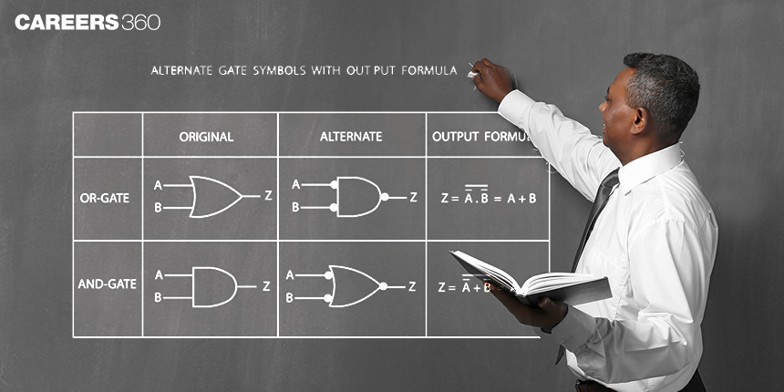
JEE Main, NEET: Logic Gate Made Easy
The topic Logic Gate constitutes less than 10 per cent of the Electronic Devices unit. But from this small portion,we selected one question for each year from 2017-21 for NEET. For JEE Main as well the questions from this topic are regularly repeated. This tells us that Logic Gates is an important topic for both the entrance exams. So let’s take a look at the concepts of logic gates that need to be studied for NEET or JEE Main.
Logic Gate
Logic gates are fundamental blocks of a digital system. There are three basic gates - AND, OR and NOT gates. Also two universal gates NAND and NOR are discussed in the unit Electronic Devices. The questions in the NEET are based on these five logic gates. The input and output of the logic gates can occur in 1 and 0 or High and Low. The truth table shows the output of the logic circuit for various combinations of the inputs. Each basic gate is discussed with its respective truth tables.
Also Read| Why You Need To Draw Boundaries With Your Teenage Child
AND Gate
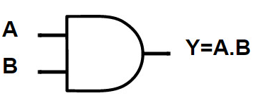 AND Gate
Output Y=A.B
AND gate can have two or more inputs with a single output. The output is High(1) only when all the inputs are High(1).
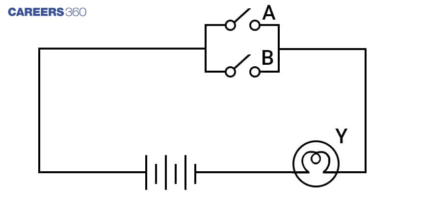
Equivalent Circuit Of AND Gate
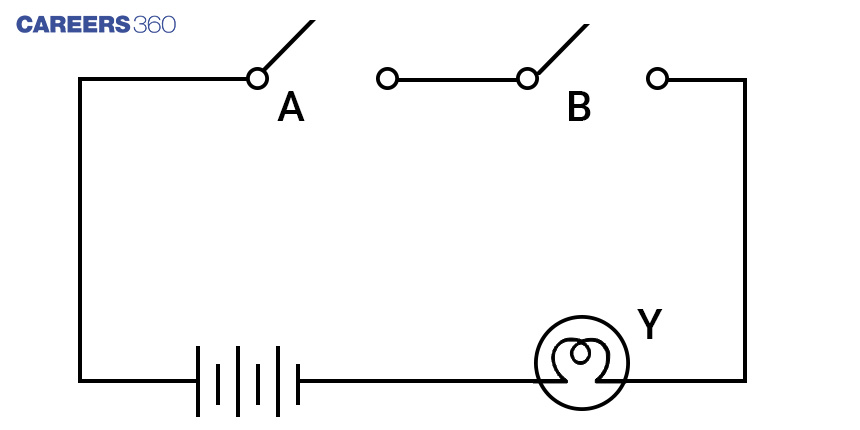 Equivalent Circuit Of AND Gate
The bulb Y glows only when both switches are closed. That is both A and B are 1. In all the other cases the bulb does not glow as the circuit is incomplete.
Truth Table Of AND Gate
Inputs | Output | |
A | B | Y |
0 | 0 | 0 |
0 | 1 | 0 |
1 | 0 | 0 |
1 | 1 | 1 |
Truth Table For Bulb And Switch Arrangement
Switches | Output | |
A | B | Bulb |
Open | Open | OFF |
Open | Closed | OFF |
Closed | Open | OFF |
Closed | Closed | ON |
OR Gate
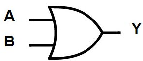 OR Gate
Output Y=A+B
OR gate can have two or more inputs with an only single output. The output is Low (0) only when all the inputs are Law(0).
The Equivalent Circuit Of OR Gate
 Equivalent Circuit Of OR Gate
When any of the switches A or B or both are closed the bulb will glow. The bulb will be off when both the switches are open.
Truth Table Of OR GATE
Inputs | Output | |
A | B | Y |
0 | 0 | 0 |
0 | 1 | 1 |
1 | 0 | 1 |
1 | 1 | 1 |
The truth table for the circuit arrangement can be easily made by replacing 0 with open switch and 1 with closed switch here. Try yourself and find out when the bulb will be ON(Glow).
Also Read| NEET Physics: Five-year Analysis, Most Asked Chapters And Concepts
Confused between CGPA and Percentage?
Get your results instantly with our calculator!
💡 Conversion Formula used is: CGPA = Percentage / 9.5
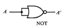
NOT Gate
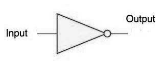 NOT Gate
Output ![]()
Also Y can be represented as Y=A’
NOT gate has only one input and one output. NOT gate is known as an inverter. The output of the NOT gate is always the complement of the input.
Equivalent Circuit Of NOT GATE
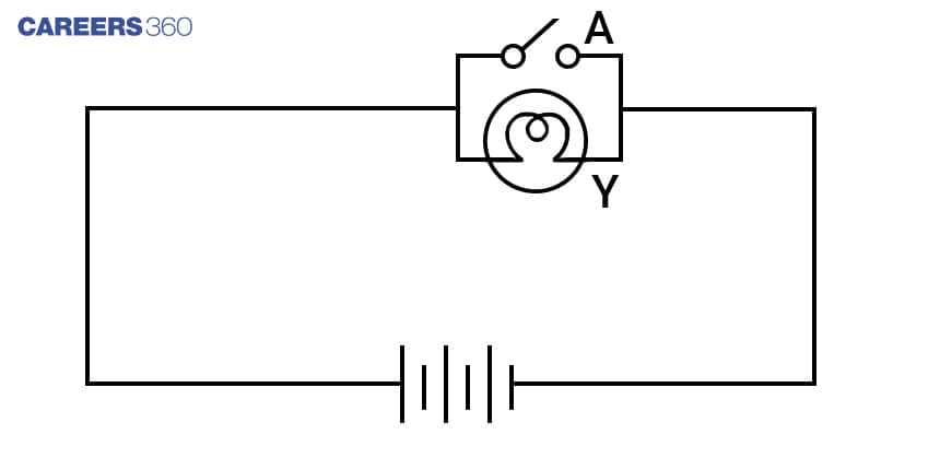 Equivalent Circuit Of NOT Gate
When the switch is open the bulb will glow. When the switch is closed the bulb is not a part of the circuit and it will remain off.
Truth Table Of NOT Gate
Input | Output |
A | Y |
0 | 1 |
1 | 0 |
Universal gates is to be discussed next. But before going to it let's have a look at some important relations.
De Morgan's Law -
A and B are input.
1) ![]()
2) ![]()
3) ![]()
4) ![]()
Some Important Relations
![]()
![]()
![]()
![]()
![]()
![]()
![]()
![]()
Universal Gates
Using universal gates we can implement any other basic Gates or Boolean function. NAND and NOR gates are universal gates. Let's have a look at the truth table for these two universal gates.
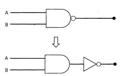
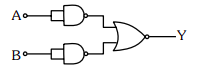
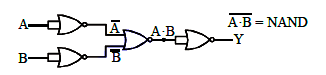
NAND GATE
NAND gate is the combination of AND gate and NOT gate.
 NAND Gate
Output ![]()
Truth Table For NAND Gate
Inputs | Output | |
A | B | Y |
0 | 0 | 1 |
0 | 1 | 1 |
1 | 0 | 1 |
1 | 1 | 0 |
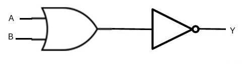
NAND gate is nothing but the inverted OR. Also from Demorgan's theorem, we know that
![]()
So the NAND gate can also be represented as -
Y=![]()
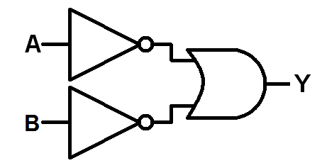
Here we see that the NAND gate is equivalent to bubbled OR. Also a bubbled NAND gate is equivalent to an OR gate.
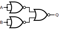
NOR Gate
NOR gate is the combination of OR gate and NOT gate.
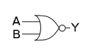
![]()
 NOR Gate
Truth Table For NOR Gate
Inputs | Output | |
A | B | Y |
0 | 0 | 1 |
0 | 1 | 0 |
1 | 0 | 0 |
1 | 1 | 0 |
NOR gate is nothing but an inverted AND. Also from Demorgan's theorem, we know that
![]()
So the NOR gate can be represented as-
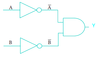
Y= ![]()
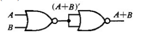
We can tell that the NOR gate is equivalent to bubbled AND. That is A’.B’=(A+B)’
. Also bubbled NOR is equivalent to AND gate. That is
![]()

Here the output Y=A.B
Questions based on this are asked in JEE Main 2009 and NEET 2020
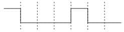
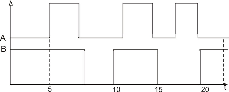
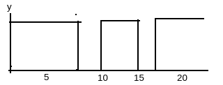
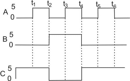
JEE Main 2009 Question: The logic circuit shown below has the input waveforms 'A' and 'B' as shown. Find the correct output waveform.

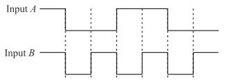
Solution: The given logical circuit is a bubbled NOR gate which is equivalent to AND gate. So the output will be HIGH when both the inputs are High. From the above-given graph it is clear that both the outputs are High in two cases only. So the output will be
And the NEET 2020 question was to find the truth table of the given logic circuit in the above question. So the truth table will be equivalent to that of an AND gate.
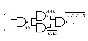
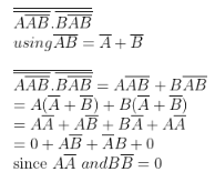
Realization Of Basic Gates Using Universal Gates
Here the term realization means how to implement a basic gate or boolean expression using the combination of only a single type of universal gate. That is either only NAND or NOR to get a desired output. Let us see some common examples.
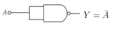
Realization Of NOT Gate Using NAND Gate
Realizing AND Gate Using NAND Gate
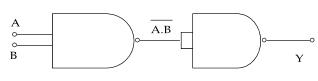
![]()
Y = A.B represents the AND gate. This was a question in JEE Main 2014
Realization Of OR Gate Using NAND Gate
From De Morgan's law
![]()
The above circuit is nothing but the bubbled NAND gate, which is equivalent to OR gate
This was a question in JEE Main 2010 and JEE Main, 2020 and 2021
JEE Main 2020 Question: Identify the correct o/p signal Y in the given combination of gates (as shown) for the given I/P A and B
The given circuit is nothing but the bubbled NAND, which is equivalent to an OR gate. So the output will be LOW when both the inputs are LOW. In all other cases, the output will be High.
So the output graph will look like this -
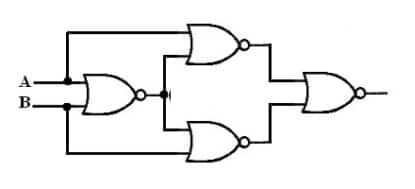
Realization Of NOR Gate Using NAND Gate
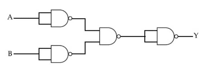
The above circuit represents a bubbled NAND given to an inverter. Bubbled NAND is nothing but OR gate. An OR gate given to the inverter is the NOR gate. JEE Main 2021 had a question to identify the truth table of the above circuit
Realization Of NOT Gate Using NOR Gate
Realization Of AND Gate Using NOR Gate
This logic circuit is nothing but the bubbled OR gate. The same is asked in JEE Main 2021. But the first two inverters (NOT gate) are realized using NAND gate.
Please read the question given below.
Question:
Identify the logic operation carried out.
Solution: AND gate(bubbled OR)
Realization Of OR Gate Using NOR Gate
![]()
((A+B)’ )’=A+B since ![]() . The sign ‘ represents compliment
. The sign ‘ represents compliment
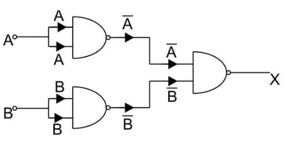
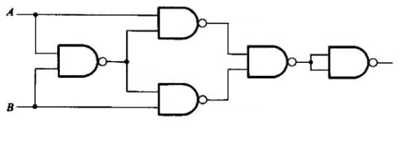
Realization Of NAND Gate Using NOR Gate
The above logic circuit is nothing but the output of bubbled NOR (AND) is given to an inverter gate. This was a question in JEE Main 2021.
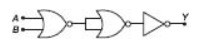
Some Familiar Logic Operations Using Universal Gates
XOR
XOR output is given by the Boolean expression ![]() . This function can be realized using different combinations of gates. The realization of A’B+AB’ using universal gates is discussed here.
. This function can be realized using different combinations of gates. The realization of A’B+AB’ using universal gates is discussed here.
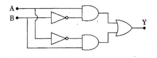
XOR Using NAND Gate
 XOR Using NAND
So we got the output AB’+A’B
Truth Table For A’B+AB’
Input A | Input B | Output |
0 | 0 | 0 |
0 | 1 | 1 |
1 | 0 | 1 |
1 | 1 | 0 |
XOR Using NOR Gate
 XOR Using OR
XNOR
XNOR output is ![]()
Truth Table For AB+A’B’
Input A | Input B | Output |
0 | 0 | 1 |
0 | 1 | 0 |
1 | 0 | 0 |
1 | 1 | 1 |
XNOR Using NAND Gate
 XNOR Using AND
The output of the combination will be ![]()
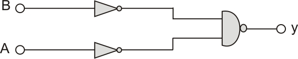
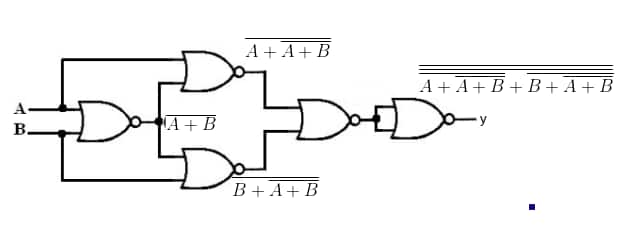
XNOR Using NOR Gate
The output of the combination will be ![]() . This was a question in JEE Main 2021. The question was to find the truth table of the above circuit.
. This was a question in JEE Main 2021. The question was to find the truth table of the above circuit.
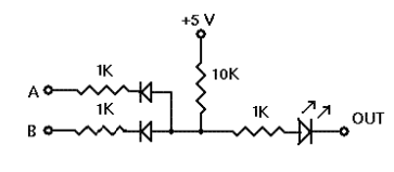
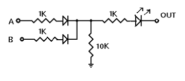
Diode Circuits For AND And OR Gate
AND Gate
OR Gate
Study all the basic and universal logic gates discussed, and for combinations of logic gates apply Demorgan's theorem or make a truth table to get the output.
But if you familiarise yourself with the above logic circuits it will be helpful to save time during the examination. You can arrive at the solutions by simply observing the circuits.
Practice Questions
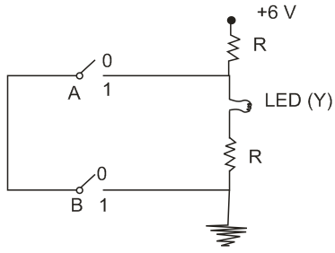
NEET 2017
The given electrical network is equivalent to
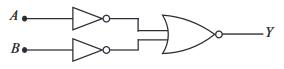
NEET 2018
In the combination of the following gates the
output Y can be written in terms of inputs A and B as
NEET 2019
The Boolean operation represented by the circuit diagram drawn is:
NEET 2020
For the logic circuit shown, the truth table is:
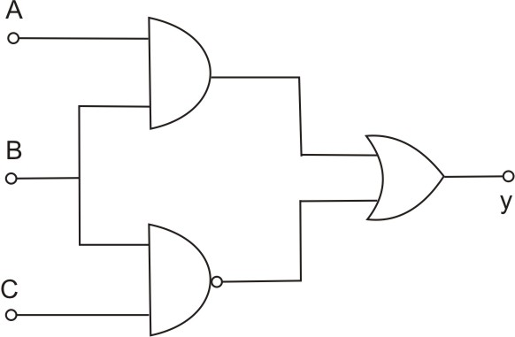
NEET 2021
For the given circuit the input digital signals are applied at the terminals A, B and C, What would be the output at terminal y?
Upcoming School Exams

Certifications By Top Providers
Explore Top Universities Across Globe
Applications for Admissions are open.
Study at a world-renowned UK university in India | Admissions open for UG & PG programs.
Victoria University, Delhi NCR
ApplyApply for UG & PG programmes from Victoria University, Delhi NCR Campus
Illinois Tech Mumbai
ApplyAdmissions open for UG & PG programs at Illinois Tech Mumbai
University of Aberdeen Mumbai
ApplyApply for UG & PG courses at University of Aberdeen, Mumbai Campus
University of York, Mumbai
ApplyUG & PG Admissions open for CS/AI/Business/Economics & other programmes.
University of Bristol, Mumbai Enterprise Campus
ApplyBristol's expertise meets Mumbai's innovation. Admissions open for UG & PG programmes
News and Notifications
Never miss update
Get timely updates directly to your inbox. Stay informed!