Careers360 Logo
Difference Between Zener Breakdown and Avalanche Breakdown

Difference Between Zener Breakdown and Avalanche Breakdown

Edited By Team Careers360 | Updated on Jul 02, 2025 05:06 PM IST

In this article we will understand in detail about zener breakdown and avalanche breakdown, what is the breakdown voltage of zener diodes? How does the avalanche breakdown in a diode occur when we apply the reverse voltage? What is zener breakdown? What is avalanche breakdown? And the difference between zener breakdown and avalanche breakdown. Breakdown means interruption or collapse in the system.

This Story also Contains
  1. What Is Avalanche Breakdown and Explain
  2. What Is Zener Breakdown and Explain
  3. Zener Breakdown and Avalanche Breakdown Difference:
  4. Important Related Topics

What Is Avalanche Breakdown and Explain

Avalanche breakdown definition: It is an occurrence that happens when the high reverse voltage is applied across the lightly doped P-N junction diode.

Now let us understand how the avalanche breakdown in a diode occurs when we apply the reverse voltage.

 Avalanche breakdown in PN junction

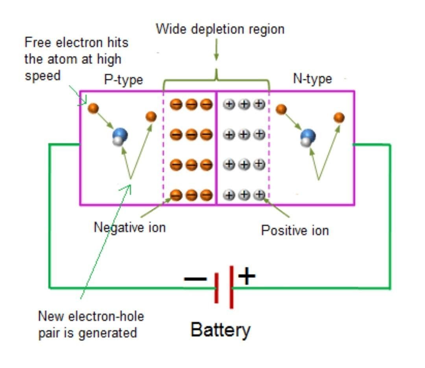
Now we know that in reverse bias conditions, the electric current that we are getting is due to the minority charge carriers. So in the reverse bias, as we intensify the applied reverse voltage, the thickness of the depletion region will intensify, and, due to that the immobile ions in this depletion region will also increase. So because of the inclination of the immobile ions, the electric field in the depletion region will become stronger and due to this stronger electric field, the minority charge carriers which are in the surrounding area to this depletion region will get accelerated.

But after the applied voltage stretches to the breakdown voltage of the silicon diode then the kinetic energy that is extended by these charge carriers will knock off the bound of the silicon atom. In the case of crystal level, accelerated electrons may collide with the silicon atom and when it has enough kinetic energy then it can knock out a bound charge or the valence charge of this atom. Now we have two free electrons under the influence of the Electric field. Now these two electrons can collide with the two more atoms and they can knock out the two more electrons.

Similarly, now these four electrons will again collide with the four more atoms and they can knock out the four more electrons. Thus due to this collision, the number of free charge carriers in the depletion region will intensify significantly. And because of this intensification in these charge carriers, we will see an abrupt hype in the reverse saturation current. So this effect is known as the Avalanche breakdown effect and the voltage after which it occurs is known as the Avalanche breakdown voltage.

We have seen this Avalanche breakdown is due to the impact ionization, meaning that the high energy charged particles can knock out the bound electrons from the silicon atom, and in this way, it creates the electron-hole pair. So for the normal diode, this region of operation should be avoided because when the applied voltage is more than this breakdown voltage then the diode starts conduct, citing in the reflection-holen also. Moreover, if there is no current limiting resistor in series with this diode then due to the very large current or very high power dissipation this diode may get damaged.

So for the normal diode, this region of operation should be avoided but some diodes are meant to be used in this breakdown region and this diode is known as the zener diode. But in Zener diodes, the breakdown, mechanism is different from the avalanche effect in diodes. So now let us understand what exactly the zener breakdown mechanism is.

What Is Zener Breakdown and Explain

Zener Breakdown

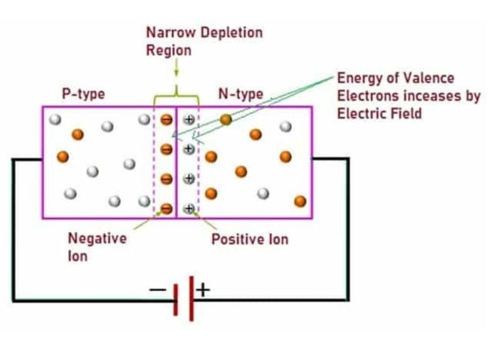
Zener breakdown definition: It is an occurrence that happens when a low reverse voltage is applied in a heavily doped P-N junction diode.

The P and N type regions of the Zener diode are heavily doped meaning that the number of impurity atoms in these p and n regions will be more due to the number of free charge carriers in both regions will be more. So due to this heavy doping the width of the depletion region will be much narrower compared to the normal diode because now when the electron diffuses from the n side to the p side then it will get recombined very much near to the junction itself. In addition to that, due to this heavy doping, this small depletion area will have a greater number of immovable ions matched to the normal diode.

So due to this the built-in electric field inside this depletion region will be much stronger and when this diode is in reverse bias then the external electric field will also get added with this built-in electric field and due to that the electric field in this depletion region will become very strong. And at one particular voltage, it will become so strong that it can knock out the bound electrons of these silicon atoms. So due to this very strong electric field, many charge carriers are generated and because of the very narrow depletion region they can tunnel through it and they can reach the other side of the depletion region.

So because of the very high electric field, many charge carriers are produced in this depletion region and current starts flowing rapidly in the reverse direction. This effect is called the zener breakdown effect and the voltage beyond which it takes place is called the zener breakdown Voltage. However, the zener effect is seen at the lower breakdown voltages.

shows breakdown regionshows avalanche and zener breakdown

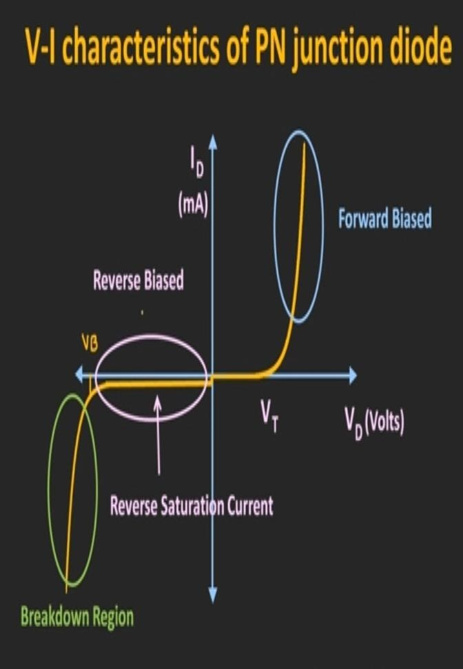
From the graph, we observe that even if we increase the applied Voltage beyond the zener voltage then the Voltage across the diode will almost remain constant. And only the current through the diode will increase. , So because of this property, the zener diode is used as a voltage regulator in many appliances.

Till now we have studied zener and avalanche breakdown. Now let us understand the difference between avalanche and zener breakdown.

Also Read:

Background wave

Zener Breakdown and Avalanche Breakdown Difference:

The difference between avalanche breakdown and zener breakdown is given below:

  • Difference based on doping of diode:
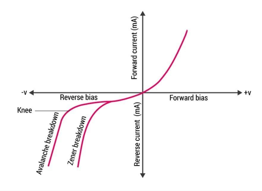
    Avalanche breakdown in a semiconductor diode occurs when the diodes are lightly doped whereas zener breakdown occurs when the diode is heavily doped.
  • Difference based on the process:
    The avalanche breakdown effect occurs due to the impact ionization whereas the Zener breakdown effect occurs due to the strong electric field (quantum tunneling).
  • Difference based on the voltages:
    The avalanche breakdown effect is seen at higher breakdown voltages (typically, higher than 6V) whereas the Zener breakdown effect is seen at lower breakdown voltages (typically, less than 4V).
  • Difference based on temperature coefficient:
    When the avalanche breakdown effect is predominant, the temperature of breakdown voltage is positive, meaning that as the temperature increases the breakdown voltage will increase whereas if the zener breakdown effect is predominant then the temperature coefficient of breakdown voltage is negative, meaning that as the temperature increases the breakdown voltage will reduce.
NEET Highest Scoring Chapters & Topics
This ebook serves as a valuable study guide for NEET exams, specifically designed to assist students in light of recent changes and the removal of certain topics from the NEET exam.
Download E-book

Important Related Topics

Forward Bias P-N Junction

In case of forward bias, the positive station of the series is connected to the P side and the negative station of the series is connected to the N side.

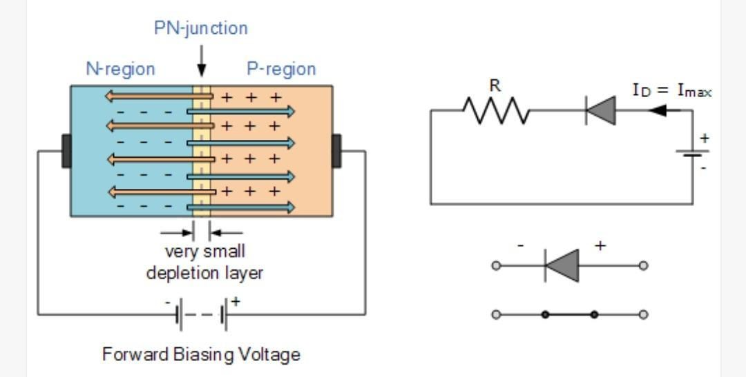
In the case of forward bias, the positive station of the series is connected to the P side and the negative station of the series is connected to the N side. In this forward bias condition, the external electric field is in the opposite direction to the built-in electric field, and due to that the affected electric field at the junction will reduce. So in the forward condition, the electron in the n-type region and the holes in the p-type region will get pushed toward the junction. So because of that the thickness of the depletion region will lessen. So the operational resistance that is accessible by the depletion region will also decrease. When the functional voltage is more than the barrier potential of this PN junction then the resistance occupied by the depletion region is insignificant. As we increase the externally applied biasing, the voltage in the circuit will increase.

Reverse Bias P-N Junction

Reverse bias PN Junction

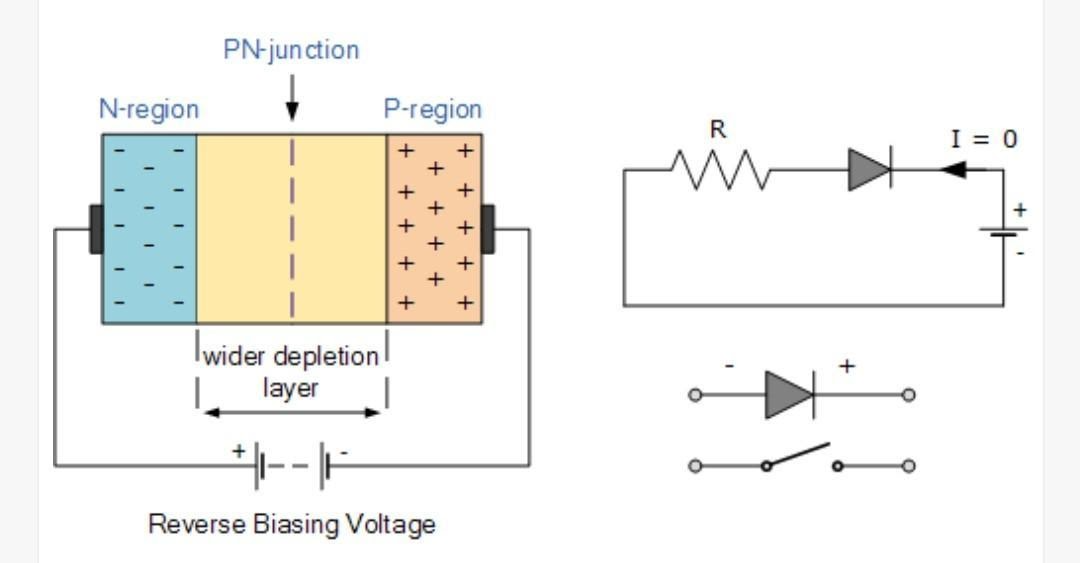
In the reverse bias condition, the negative station of the series is connected to the P side and the positive station of the series is connected to the N side. So in this condition, the electrons which are mainstream carriers in this N-type region will get engrossed toward the positive terminal of the battery and similarly, the holes on the P-side region will get engrossed toward the negative terminal of the battery. And because of that other ions will get generated near the junction. So we can say that the thickness of the depletion region will intensify.

So in the reverse bias condition, as we increase the reverse bias voltage the thickness of the depletion region will additionally intensify. Due to that virtually, there is no flow of current due to the majority of carriers. But in the case due to the built-in electric field, minority carriers in both regions will be able to cross this depletion region. However, the minority carriers are very less in comparison to the majority carriers. So the flow of current that exists in this reverse bias condition is known as reverse saturation current. The reverse saturation current does not change much even if we increase the reverse bias voltage but there is a limit to the maximum reverse voltage that can be applied to this PN junction.

So, if we continuously increase this reverse voltage then we will reach a point which is known as the breakdown voltage of the diode. After the breakdown voltage for the diode, a lot of minority carriers will be seen at the depletion region and unexpectedly the diode behaves very profoundly. This effect is known as the Avalanche effect in diodes. Now let us study in detail about zener and avalanche breakdown.

Frequently Asked Questions (FAQs)

1. What is the breakdown voltage of a zener diode?

Breakdown voltage of the zener diode is less than 4V.

2. Define avalanche.

Avalanche means the sudden occurrence or fall of something.

3. How do the temperature coefficient of zener diode and avalanche diode differ?

The temperature coefficient of avalanche breakdown voltage is positive whereas the temperature coefficient of zener breakdown voltage is negative.

4. What is the breakdown voltage of avalanche breakdown?

The breakdown voltage of avalanche breakdown is higher than 6V.

5. Why is the zener diode setup reverse biased?

Because in reverse biasing the potential at the junction increases.

6. What is the impact of junction capacitance on Zener and avalanche breakdown?
Junction capacitance affects both types of breakdown, but its impact is more significant in avalanche breakdown. In Zener diodes, the narrow depletion region results in higher capacitance, but it doesn't significantly affect the breakdown mechanism. In avalanche devices, the capacitance can influence the speed of breakdown and recovery, affecting their high-frequency performance and switching characteristics.
7. How do Zener and avalanche breakdown mechanisms influence the design of voltage reference circuits?
Zener breakdown is often preferred for voltage reference circuits due to its lower voltage operation and sharper breakdown characteristic. This allows for more precise voltage control. Avalanche breakdown, occurring at higher voltages, is sometimes used for high-voltage references. The temperature coefficients of each mechanism are also considered in design, with some circuits combining both effects for temperature compensation.
8. Can the type of breakdown in a p-n junction be controlled or engineered?
Yes, the type of breakdown can be engineered through careful control of doping profiles and junction design. Higher doping concentrations and abrupt junctions favor Zener breakdown, while lower doping and gradual junctions promote avalanche breakdown. Junction depth, geometry, and even material choice can be tailored to achieve the desired breakdown characteristics for specific applications.
9. How do Zener and avalanche breakdown affect the reverse recovery time of a diode?
Zener breakdown generally results in faster reverse recovery times compared to avalanche breakdown. This is because Zener breakdown involves fewer charge carriers and occurs in a more localized region. Avalanche breakdown, involving a larger number of carriers spread over a wider region, typically leads to longer reverse recovery times due to the need to clear these excess carriers.
10. How do Zener and avalanche breakdown mechanisms affect the reliability and lifespan of semiconductor devices?
Both breakdown mechanisms can impact device reliability, but in different ways. Zener breakdown, being a quantum tunneling effect, generally causes less physical stress on the device. Avalanche breakdown, involving high-energy collisions, can potentially cause more cumulative damage over time. However, when properly managed, both can be used reliably. Devices designed to operate in breakdown (like Zener diodes) are engineered to withstand these effects for extended periods.
11. What is the significance of the "multiplication factor" in avalanche breakdown?
The multiplication factor in avalanche breakdown represents the number of electron-hole pairs created by a single carrier through impact ionization. It increases with the electric field strength. A higher multiplication factor leads to a more rapid increase in current, resulting in a sharper breakdown characteristic. This factor is crucial in understanding the avalanche process and designing devices that utilize it.
12. Why is avalanche breakdown sometimes described as a "snowball effect"?
Avalanche breakdown is described as a "snowball effect" because of its self-amplifying nature. As electrons gain enough energy to cause impact ionization, they create more electron-hole pairs. These new carriers are then accelerated, causing further ionization, leading to an exponential increase in current. This cascading effect is similar to a snowball rolling down a hill, growing larger as it collects more snow.
13. What is the role of minority carriers in Zener and avalanche breakdown?
Minority carriers play a minimal role in Zener breakdown, as it primarily involves electron tunneling through the energy barrier. In avalanche breakdown, minority carriers are crucial. They are accelerated by the electric field and collide with lattice atoms, creating electron-hole pairs. These newly created carriers further accelerate and create more pairs, leading to the avalanche effect.
14. How does the carrier lifetime affect Zener and avalanche breakdown?
Carrier lifetime has a more significant impact on avalanche breakdown than on Zener breakdown. In avalanche breakdown, longer carrier lifetimes allow more time for impact ionization, potentially lowering the breakdown voltage. For Zener breakdown, which primarily depends on tunneling, carrier lifetime has minimal effect. However, it can influence the device's recovery time after breakdown in both cases.
15. How does the crystal structure of the semiconductor material influence Zener and avalanche breakdown?
Crystal structure affects both breakdown mechanisms, but more significantly avalanche breakdown. In Zener breakdown, the crystal structure influences the tunneling probability to some extent. For avalanche breakdown, the crystal structure impacts carrier mobility and mean free path, which are crucial for impact ionization. Materials with different crystal structures (e.g., silicon vs. gallium arsenide) can exhibit different breakdown characteristics due to these factors.
16. Why is Zener breakdown sometimes called "internal field emission"?
Zener breakdown is called "internal field emission" because it involves electrons being emitted from the valence band to the conduction band within the semiconductor material, similar to field emission in vacuum tubes. The strong electric field in the narrow depletion region causes this "emission" by enabling electrons to tunnel through the energy barrier, hence the term "internal field emission."
17. How does the breakdown voltage change with the width of the depletion region?
As the depletion region width increases, the breakdown voltage generally increases. For Zener breakdown, a wider depletion region reduces the probability of quantum tunneling, requiring higher voltages. In avalanche breakdown, a wider region means electrons need to travel further to gain enough energy for impact ionization, also necessitating higher voltages.
18. Can Zener breakdown occur in wide-bandgap semiconductors?
Zener breakdown is less likely to occur in wide-bandgap semiconductors. The wider bandgap makes it more difficult for electrons to tunnel through the energy barrier. In these materials, avalanche breakdown is more common. However, with extremely heavy doping and very narrow junctions, Zener-like tunneling effects can still be observed even in some wide-bandgap materials.
19. Why are Zener diodes typically used for voltage regulation instead of avalanche diodes?
Zener diodes are preferred for voltage regulation because they operate at lower voltages and have a sharper knee in their I-V characteristics. This makes them more suitable for precise voltage control. Additionally, Zener breakdown's negative temperature coefficient can be balanced with the positive temperature coefficient of the diode's series resistance, resulting in a more stable reference voltage.
20. How does the electric field strength in the depletion region differ between Zener and avalanche breakdown?
In Zener breakdown, the electric field strength is extremely high (>107 V/cm) due to the narrow depletion region, enabling quantum tunneling. For avalanche breakdown, the field strength is lower but still significant (105-106 V/cm), sufficient to accelerate electrons to energies that can cause impact ionization. The field strength directly relates to the doping concentration and junction width.
21. What is the fundamental difference between Zener breakdown and avalanche breakdown?
Zener breakdown occurs in heavily doped p-n junctions with a narrow depletion region, typically at low reverse voltages (<5V). It's caused by quantum tunneling of electrons. Avalanche breakdown happens in lightly doped junctions with wider depletion regions, at higher reverse voltages (>5V), due to impact ionization. The key difference is the underlying mechanism and the voltage at which they occur.
22. Why does Zener breakdown occur at lower voltages compared to avalanche breakdown?
Zener breakdown occurs at lower voltages because it relies on quantum tunneling, which becomes significant in heavily doped, narrow junctions. The narrow depletion region allows electrons to tunnel through the potential barrier more easily. Avalanche breakdown requires higher voltages to accelerate electrons to energies sufficient for impact ionization in wider depletion regions.
23. Can both Zener and avalanche breakdown occur simultaneously in a single device?
Yes, in some cases, both mechanisms can contribute to breakdown. This typically occurs in moderately doped junctions with reverse voltages around 5-7V. The total current is then a combination of tunneling current (Zener effect) and impact ionization current (avalanche effect). However, one mechanism usually dominates.
24. How does temperature affect Zener and avalanche breakdown?
Zener breakdown has a negative temperature coefficient, meaning the breakdown voltage decreases with increasing temperature. Avalanche breakdown has a positive temperature coefficient, so its breakdown voltage increases with temperature. This difference is due to their distinct underlying mechanisms and how they're affected by lattice vibrations and carrier mobility.
25. How does the doping concentration affect the type of breakdown in a p-n junction?
Higher doping concentrations lead to narrower depletion regions, favoring Zener breakdown. Lower doping concentrations result in wider depletion regions, promoting avalanche breakdown. The doping level directly influences the electric field strength and depletion region width, determining which breakdown mechanism dominates.
26. How does the noise characteristic differ between Zener and avalanche breakdown?
Zener breakdown generally produces less noise compared to avalanche breakdown. This is because Zener breakdown involves a more uniform, quantum tunneling process. Avalanche breakdown, involving discrete collision events and multiplication of carriers, tends to be noisier. This difference in noise characteristics can be important in sensitive electronic applications.
27. How does the I-V characteristic curve differ between Zener and avalanche breakdown?
The I-V curve for Zener breakdown typically shows a sharper "knee" and a more abrupt increase in current at the breakdown voltage. Avalanche breakdown often exhibits a softer knee and a more gradual increase in current. The Zener curve tends to be more vertical in the breakdown region, while the avalanche curve may have a slight slope, reflecting the different underlying mechanisms.
28. What role does the depletion region's electric field profile play in determining the type of breakdown?
The electric field profile in the depletion region is crucial in determining the breakdown type. Zener breakdown requires an extremely high, localized electric field, typically found in abrupt, heavily doped junctions. Avalanche breakdown occurs in more uniform, moderately high electric fields over a wider region. The field profile, shaped by doping concentration and junction geometry, directly influences which mechanism dominates.
29. What is the significance of the "multiplication region" in avalanche breakdown?
The multiplication region in avalanche breakdown is the area where impact ionization occurs most intensely. It's typically the high-field region of the depletion layer. The size and characteristics of this region determine the avalanche multiplication factor and the sharpness of the breakdown. Understanding and controlling this region is crucial for designing devices that utilize avalanche effects, such as avalanche photodiodes.
30. How do Zener and avalanche breakdown mechanisms affect the switching speed of devices?
Zener breakdown generally allows for faster switching speeds compared to avalanche breakdown. This is because Zener breakdown involves fewer carriers and occurs in a more localized region, allowing for quicker depletion of excess charges. Avalanche breakdown, involving more carriers over a larger area, typically results in slower switching speeds due to the time required to clear the excess carriers from the wider depletion region.
31. What is the relationship between the breakdown voltage and the doping concentration in Zener and avalanche breakdown?
For Zener breakdown, the breakdown voltage decreases with increasing doping concentration. This is because higher doping narrows the depletion region, enhancing the tunneling probability. In avalanche breakdown, the relationship is more complex. Initially, higher doping reduces the breakdown voltage by increasing the electric field. However, extremely high doping can lead to a transition to Zener breakdown, causing a different voltage-doping relationship.
32. How do Zener and avalanche breakdown mechanisms influence the design of ESD (Electrostatic Discharge) protection circuits?
Both mechanisms are utilized in ESD protection circuits, but in different ways. Zener breakdown is often used for low-voltage protection due to its sharp turn-on characteristic and lower operating voltage. Avalanche breakdown is employed for higher voltage protection. The choice depends on the voltage range and speed requirements of the protection circuit. Some designs combine both effects for comprehensive protection across different voltage ranges.
33. Can Zener and avalanche breakdown occur in forward-biased junctions?
Zener and avalanche breakdown are primarily reverse-bias phenomena. In forward bias, the potential barrier is lowered, allowing for normal current flow without breakdown. However, in certain specialized structures or under extreme forward bias conditions, effects similar to avalanche multiplication can occur. These are not typically classified as breakdown but as other phenomena like punch-through or reach-through effects.
34. How does the presence of impurities or defects in the semiconductor affect Zener and avalanche breakdown?
Impurities and defects can significantly influence both breakdown mechanisms. For Zener breakdown, they can create localized high-field regions that enhance tunneling probability. In avalanche breakdown, impurities and defects can act as generation-recombination centers, affecting the carrier multiplication process. Generally, these imperfections can lower the breakdown voltage and make it less uniform across the device, potentially impacting reliability and performance.
35. What is the importance of the "critical field strength" in avalanche breakdown?
The critical field strength in avalanche breakdown is the minimum electric field required to initiate impact ionization. When the field in the depletion region reaches this critical value, electrons gain enough energy between collisions to ionize lattice atoms, starting the avalanche process. This parameter is crucial in determining the avalanche breakdown voltage and is influenced by the semiconductor material properties and doping profile.
36. How do Zener and avalanche breakdown mechanisms affect the reverse leakage current in a p-n junction?
Before breakdown, Zener and avalanche mechanisms contribute differently to reverse leakage current. Zener effect can cause a slight increase in leakage current due to tunneling, even before full breakdown. Avalanche effects typically don't significantly affect leakage until near the breakdown voltage. Post-breakdown, both mechanisms lead to a sharp increase in current, but Zener breakdown often results in a more abrupt rise compared to avalanche breakdown.
37. What is the role of carrier velocity saturation in avalanche breakdown?
Carrier velocity saturation plays a crucial role in avalanche breakdown. As the electric field increases, carrier velocity initially increases linearly but eventually saturates due to increased scattering. This saturation affects the energy carriers can gain between collisions, influencing the onset of impact ionization. It's a key factor in determining the critical field strength and, consequently, the avalanche breakdown voltage in high-field regions.
38. How do Zener and avalanche breakdown mechanisms influence the choice of materials in semiconductor device design?
The breakdown mechanism influences material choice based on the desired device characteristics. Materials with smaller bandgaps are more prone to Zener breakdown at lower voltages, making them suitable for low-voltage reference diodes. Wide-bandgap materials, favoring avalanche breakdown, are often chosen for high-voltage or high-power applications. The material's impact ionization coefficients and critical field strength are also considered for devices utilizing avalanche effects.
39. What is the significance of the "ionization integral" in understanding avalanche breakdown?
The ionization integral is a mathematical concept used to predict the onset of avalanche breakdown. It represents the cumulative ionization effect across the depletion region. When this integral reaches unity, it indicates that each carrier entering the high-field region will, on average, create one electron-hole pair through impact ionization, leading to self-sustaining avalanche multiplication. This concept is crucial for accurately modeling and predicting avalanche breakdown behavior.
40. How do Zener and avalanche breakdown mechanisms affect the reverse recovery characteristics of power diodes?
Zener breakdown generally results in faster reverse recovery compared to avalanche breakdown. This is because Zener breakdown involves fewer excess carriers and occurs in a more localized region. Avalanche breakdown, creating more carriers over a wider area, typically leads to longer reverse recovery times. In power diodes, where fast switching is often crucial, this difference can be significant in determining the device's high-frequency performance and switching losses.
41. What is the relationship between the breakdown voltage and the temperature coefficient in Zener and avalanche breakdown?
Zener breakdown typically has a negative temperature coefficient, meaning the breakdown voltage decreases with increasing temperature. This is due to increased lattice vibrations enhancing the tunneling probability. Avalanche breakdown usually has a positive temperature coefficient, as increased temperature reduces carrier mobility, requiring higher voltages for impact ionization. Understanding these temperature dependencies is crucial for designing stable voltage reference circuits and temperature-compensated devices.
42. How do Zener and avalanche breakdown mechanisms influence the noise characteristics of voltage reference circuits?
Zener breakdown generally produces less noise compared to avalanche breakdown, making it preferable for low-noise voltage reference applications. The quantum tunneling process in Zener breakdown is more uniform and less prone to fluctuations. Avalanche breakdown, involving discrete collision events, tends to generate more noise, particularly shot noise and microplasma noise. This difference in noise characteristics is a key consideration in designing precision analog circuits.
43. What is the impact of junction geometry on Zener and avalanche breakdown?
Junction geometry significantly affects both breakdown mechanisms. For Zener breakdown, abrupt junctions with small radii of curvature enhance the local electric field, promoting tunneling at lower voltages. In avalanche breakdown, the junction geometry influences the electric field distribution and the size of the multiplication region. Planar junctions typically have higher breakdown voltages compared to curved or spherical junctions due to more uniform field distribution.
44. How do Zener and avalanche breakdown mechanisms affect the design of voltage multiplier circuits?
In voltage multiplier circuits, avalanche breakdown is more commonly utilized due to its occurrence at higher voltages. Avalanche di

Articles

Back to top